- 您現在的位置:買賣IC網 > PDF目錄373983 > ADF4251 (Analog Devices, Inc.) Dual Fractional-N/Integer-N Frequency Synthesizer PDF資料下載
參數資料
| 型號: | ADF4251 |
| 廠商: | Analog Devices, Inc. |
| 英文描述: | Dual Fractional-N/Integer-N Frequency Synthesizer |
| 中文描述: | 雙Fractional-N/Integer-N頻率合成器 |
| 文件頁數: | 12/28頁 |
| 文件大小: | 387K |
| 代理商: | ADF4251 |
第1頁第2頁第3頁第4頁第5頁第6頁第7頁第8頁第9頁第10頁第11頁當前第12頁第13頁第14頁第15頁第16頁第17頁第18頁第19頁第20頁第21頁第22頁第23頁第24頁第25頁第26頁第27頁第28頁
REV. 0
–12–
ADF4251
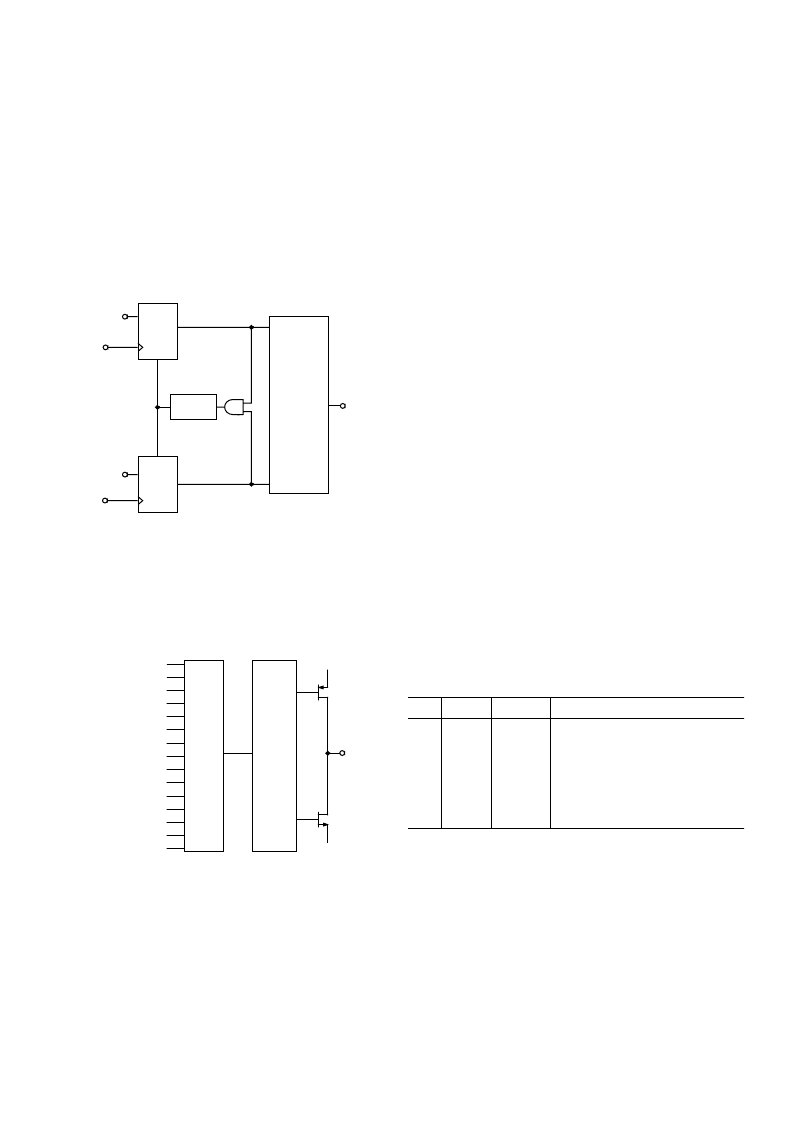
Phase Frequency Detector (PFD) and Charge Pump
The PFD takes inputs from the R counter and N counter and
produces an output proportional to the phase and frequency
difference between them. Figure 6 is a simplified schematic. The
PFD includes a delay element that controls the width of the
antibacklash pulse. This pulse ensures that there is no dead zone
in the PFD transfer function and minimizes phase noise and
reference spurs.
+IN
D1
Q1
CLR1
U1
U3
DELAY
ELEMENT
HI
UP
D2
Q2
CLR2
U2
HI
DOWN
CHARGE
PUMP
CP
–IN
Figure 6. PFD Simplified Schematic
MUXOUT and Lock Detect
The output multiplexer on the ADF4251 allows the user to
access various internal points on the chip. The state of MUXOUT
is controlled by M4, M3, M2, and M1 in the Master Register.
Table VI shows the full truth table. Figure 7 shows the MUXOUT
section in block diagram format.
LOGIC LOW
IF ANALOG LOCK DETECT
IF R DIVIDER OUTPUT
IF N DIVIDER OUTPUT
RF ANALOG LOCK DETECT
IF/RF ANALOG LOCK DETECT
IF DIGITAL LOCK DETECT
LOGIC HIGH
RF R DIVIDER OUTPUT
RF N DIVIDER OUTPUT
THREE STATE OUTPUT
RF DIGITAL LOCK DETECT
RF/IF DIGITAL LOCK DETECT
LOGIC HIGH
LOGIC LOW
MUX
CONTROL
MUXOUT
DV
DD
D
GND
Figure 7. MUXOUT Circuit
Lock Detect
MUXOUT can be programmed for two types of lock detect: digital
and analog. Digital is active high. The N-channel open-drain
analog lock detect should be operated with an external pull-up
resistor of 10 k
W
nominal. When lock has been detected, this
output will be high with narrow low going pulses.
Hardware Power-Down/Chip Enable
In addition to the software power-down methods described on
pages 21 and 22, the ADF4251 also has a hardware power-
down feature. This is accessed via the Chip Enable (CE) pin.
When this pin is Logic High, the device is in normal operation.
Bringing the CE pin Logic Low will power down the device.
When this happens, the following events occur:
1. All active dc current paths are removed.
2. The RF and IF counters are forced to their load
state conditions.
3. The RF and IF charge pumps are forced into three-state mode.
4. The digital lock detect circuitry is reset.
5. The RF
IN
and IF
IN
inputs are debiased.
6. The REF
IN
input buffer circuitry is disabled.
7. The serial interface input register remains active and capable
of loading and latching data.
Bringing the CE pin back up again to Logic High will reinstate
normal operation, depending on the software power-down settings.
Input Shift Register
Data is clocked in on each rising edge of CLK. The data is
clocked in MSB first. Data is transferred from the input register
to one of seven latches on the rising edge of LE. The destination
latch is determined by the state of the three control bits (C2, C1,
and C0) in the shift register. These are the three LSBs: DB2,
DB1, and DB0, as shown in Figure 1. The truth table for these
bits is shown in Table I. Table II shows a summary of how the
registers are programmed.
Table I. Control Bit Truth Table
C2
C1
C0
Data Latch
0
0
0
0
1
1
1
0
0
1
1
0
0
1
0
1
0
1
0
1
0
RF N Divider Reg
RF R Divider Reg
RF Control Reg
Master Reg
IF N Divider Reg
IF R Divider Reg
IF Control Reg
相關PDF資料 |
PDF描述 |
|---|---|
| ADF4251BCP | Dual Fractional-N/Integer-N Frequency Synthesizer |
| ADF4251BCP-REEL | Dual Fractional-N/Integer-N Frequency Synthesizer |
| ADF4251BCP-REEL7 | Dual Fractional-N/Integer-N Frequency Synthesizer |
| ADF4252BCP | Dual Fractional-N/Integer-N Frequency Synthesizer |
| ADF4252BCP-REEL | Dual Fractional-N/Integer-N Frequency Synthesizer |
相關代理商/技術參數 |
參數描述 |
|---|---|
| ADF4251BCP | 制造商:Analog Devices 功能描述:PLL Frequency Synthesizer Dual 24-Pin LFCSP EP |
| ADF4251BCP-REEL | 制造商:AD 制造商全稱:Analog Devices 功能描述:Dual Fractional-N/Integer-N Frequency Synthesizer |
| ADF4251BCP-REEL7 | 制造商:AD 制造商全稱:Analog Devices 功能描述:Dual Fractional-N/Integer-N Frequency Synthesizer |
| ADF4252 | 制造商:AD 制造商全稱:Analog Devices 功能描述:Dual Fractional-N/Integer-N Frequency Synthesizer |
| ADF4252BCP | 制造商:Analog Devices 功能描述:PLL Frequency Synthesizer Dual 24-Pin LFCSP EP 制造商:Rochester Electronics LLC 功能描述:1000-2500MHZ FRAC-N PLL - Bulk 制造商:Analog Devices 功能描述:IC SYNTHESIZER PLL |
發布緊急采購,3分鐘左右您將得到回復。