- 您現在的位置:買賣IC網 > PDF目錄373983 > ADF4360-7BCP (ANALOG DEVICES INC) Integrated Synthesizer and VCO PDF資料下載
參數資料
| 型號: | ADF4360-7BCP |
| 廠商: | ANALOG DEVICES INC |
| 元件分類: | 無繩電話/電話 |
| 英文描述: | Integrated Synthesizer and VCO |
| 中文描述: | TELECOM, CELLULAR, BASEBAND CIRCUIT, QCC24 |
| 封裝: | 4 X 4 MM, MO-220-VGGD-2, LFCSP-24 |
| 文件頁數: | 4/20頁 |
| 文件大小: | 336K |
| 代理商: | ADF4360-7BCP |
PRELIMINARY TECHNICAL DATA
REV. PrA 07/03
ADF4360-2
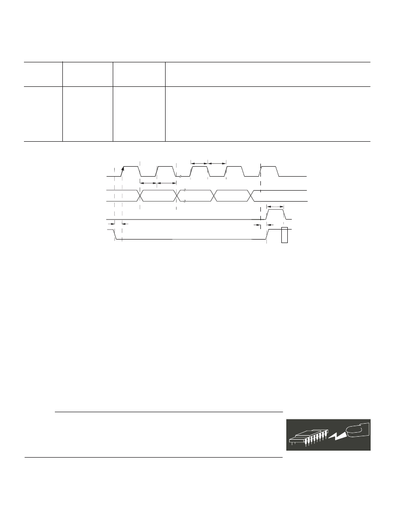
TIMING CHARACTERISTICS
–4–
CAUTION
ESD (electrostatic discharge) sensitive device. Electrostatic charges as high as 4000 V
readily accumulate on the human body and test equipment and can discharge without
detection. Although the ADF4360 family features proprietary ESD protection circuitry,
permanent damage may occur on devices subjected to high-energy electrostatic
discharges. Therefore, proper ESD precautions are recommended to avoid performance
degradation or loss of functionality.
WARNING!
ESD SENSITIVE DEVICE
Limit at
T
MIN
to T
MAX
(B Version)
Parameter
Units
Test Conditions/Comments
t
1
t
2
t
3
t
4
t
5
t
6
t
7
20
10
10
25
25
10
20
ns min
ns min
ns min
ns min
ns min
ns min
ns min
LE Set Up Time
DATA to CLOCK Set Up Time
DATA to CLOCK Hold Time
CLOCK High Duration
CLOCK Low Duration
CLOCK to LE Set Up Time
LE Pulse Width
(AV
DD
= DV
DD
= V
VCO
= +3.3V ± 10%; AGND = DGND = 0 V; 1.8V and 3V Logic Levels Used; T
A
=
T
MIN
to T
MAX
unless otherwise noted)
Figure 1. Timing Diagram
ABSOLUTE MAXIMUM RATINGS
1, 2
(
T
A
= +25°C unless otherwise noted)
AV
DD
to GND
3
...................................–0.3 V to +3.9 V
AV
DD
to DV
DD
...................................–0.3 V to +0.3 V
V
VCO
to GND......................................–0.3 V to +3.9 V
V
VCO
to AV
DD
......................................–0.3 V to +0.3 V
Digital I/O Voltage to GND..........–0.3 V to V
DD
+ 0.3 V
Analog I/O Voltage to GND..........–0.3 V to V
DD
+ 0.3 V
REF
IN
, to GND............................–0.3 V to V
DD
+ 0.3 V
OperatingTemperature Range
Maximum Junction Temperature........................+150°C
CSP
θ
JA
Thermal Impedance
(Paddle Soldered).......................................50°C/W
(Paddle Not Soldered).................................88°C/W
Lead Temperature, Soldering
Vapor Phase (60 sec)......................................+215°C
Infrared (15 sec)............................................+220°C
1. Stresses above those listed under “Absolute Maximum Ratings” may
cause permanent damage to the device. This is a stress rating only and
functional operation of the device at these or any other conditions above
those listed in the operational sections of this specification is not implied.
Exposure to absolute maximum rating conditions for extended periods
may affect device reliability.
2. This device is a high-performance RF integrated circuit with an ESD
rating of < 1kV and it is ESD sensitive. Proper precautions should be
taken for handling and assembly.
3. GND = AGND = DGND = 0V
TRANSISTOR COUNT
12543 (CMOS) and 700 (Bipolar)
t
6
t
7
CLOCK
DB23
(MSB)
DB22
DB2
DB1
(CONTROL BIT C2)
DATA
LE
LE
DB0 (LSB)
(CONTROL BIT C1)
t
2
t
3
t
4
t
5
t
1
相關PDF資料 |
PDF描述 |
|---|---|
| ADF4360-5 | Integrated Synthesizer and VCO |
| ADF4360-5BCP | Integrated Synthesizer and VCO |
| ADF4360-5BCPRL | Integrated Synthesizer and VCO |
| ADF4360-5BCPRL7 | Integrated Synthesizer and VCO |
| ADF4360-3 | Integrated Synthesizer and VCO |
相關代理商/技術參數 |
參數描述 |
|---|---|
| ADF4360-7BCPRL | 制造商:Analog Devices 功能描述:PLL Frequency Synthesizer Single 24-Pin LFCSP EP T/R |
| ADF4360-7BCPRL7 | 制造商:Analog Devices 功能描述:PLL Frequency Synthesizer Single 24-Pin LFCSP EP T/R |
| ADF4360-7BCPU1 | 制造商:Analog Devices 功能描述:PLL FREQ SYNTHESIZER SGL 24LFCSP EP - Bulk |
| ADF43607BCPZ | 制造商:ADI 功能描述:NEW |
| ADF4360-7BCPZ | 功能描述:IC SYNTHESIZER/VCO 24-LFCSP RoHS:是 類別:集成電路 (IC) >> 時鐘/計時 - 時鐘發生器,PLL,頻率合成器 系列:- 標準包裝:2,000 系列:- 類型:PLL 頻率合成器 PLL:是 輸入:晶體 輸出:時鐘 電路數:1 比率 - 輸入:輸出:1:1 差分 - 輸入:輸出:無/無 頻率 - 最大:1GHz 除法器/乘法器:是/無 電源電壓:4.5 V ~ 5.5 V 工作溫度:-20°C ~ 85°C 安裝類型:表面貼裝 封裝/外殼:16-LSSOP(0.175",4.40mm 寬) 供應商設備封裝:16-SSOP 包裝:帶卷 (TR) 其它名稱:NJW1504V-TE1-NDNJW1504V-TE1TR |
發布緊急采購,3分鐘左右您將得到回復。