- 您現在的位置:買賣IC網 > PDF目錄373983 > ADF4360-7BCP (ANALOG DEVICES INC) Integrated Synthesizer and VCO PDF資料下載
參數資料
| 型號: | ADF4360-7BCP |
| 廠商: | ANALOG DEVICES INC |
| 元件分類: | 無繩電話/電話 |
| 英文描述: | Integrated Synthesizer and VCO |
| 中文描述: | TELECOM, CELLULAR, BASEBAND CIRCUIT, QCC24 |
| 封裝: | 4 X 4 MM, MO-220-VGGD-2, LFCSP-24 |
| 文件頁數: | 9/20頁 |
| 文件大小: | 336K |
| 代理商: | ADF4360-7BCP |
PRELIMINARY TECHNICAL DATA
ADF4360-2
REV. PrA 07/03
–9–
VCO
The VCO core in the ADF4360 family uses eight overlapping
bands as shown in figure 6 to allow a wide frequency range to
be covered without a large VCO sensitivity (Kv) and resultant
poor phase noise and spurious performance.
The correct band is chosen automatically by the band select
logic at power-up or whenever the N Counter latch is updated.
It is important that the correct write sequence be followed at
power-up. This sequence is:
1) R Counter latch
2) Control latch
3) N Counter latch
During band select, which takes five PFD cycles, The VCO
Vtune is disconnected from the output of the loop filter and
connected to an internal reference voltage.
The operating current in the VCO core is programmable
in four steps, 5mA, 10mA, 15mA & 20mA. This is
controlled by bits PC1 & PC2 in the Control latch.
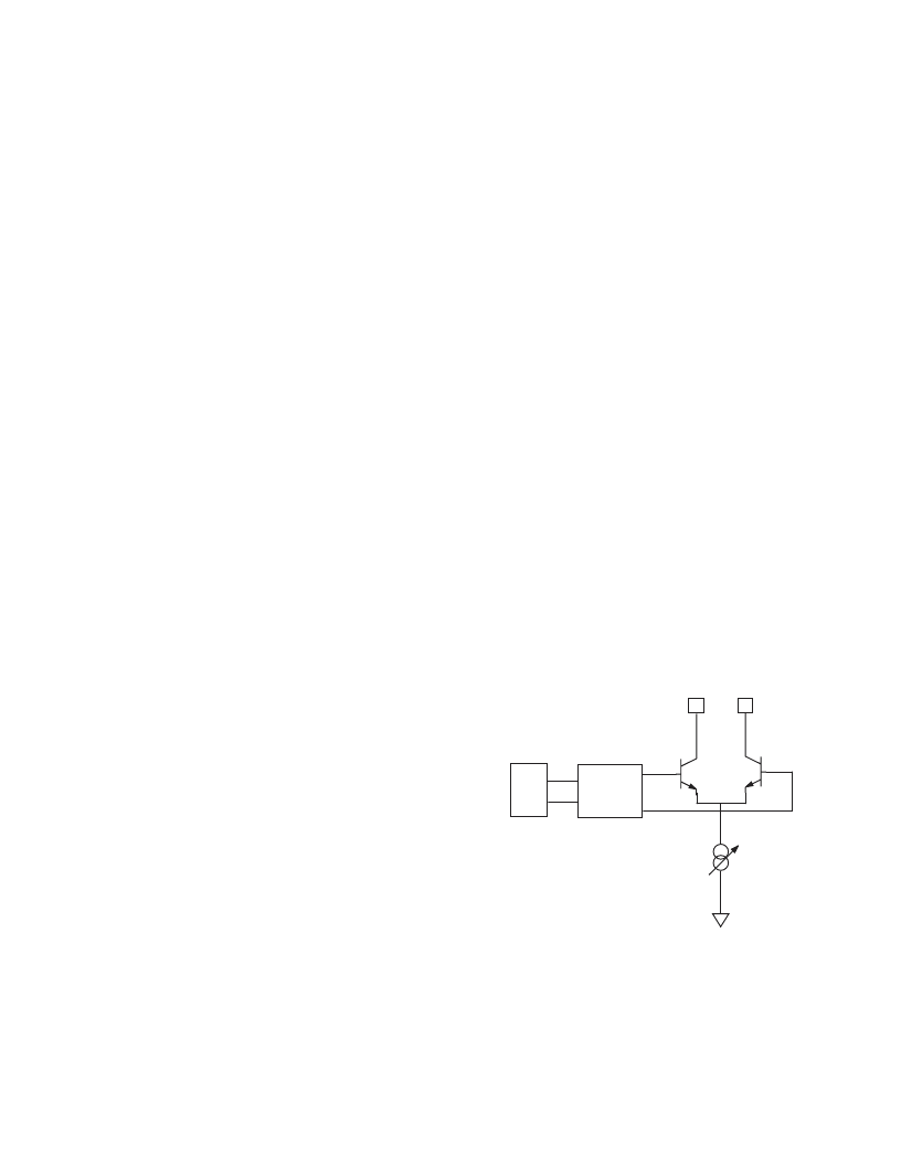
OUTPUT STAGE
The RFoutA and RFoutB pins of the ADF4360 family are
connected to the collectors of an NPN differential pair
driven by buffered outputs of the VCO as shown in figure
7. To allow the user to optimise his/her power dissipation
vs output power requirements, The tail current of the
differential pair is programmable via bits PL1 & PL2 in
the Control latch. Four current levels may be set; 3.5mA,
5mA, 7.5mA and 11mA giving output power levels of -
13dBm, -10.5dBm, -8dBm & -6dBm using a 50Ohm
resistor to Vdd and ac-coupling into a 50Ohm load.
Alternatively, both outputs can be combined in a 1+1:1
transformer or a 180 microstrip coupler. See Page 19.
If the outputs are to be used individually, then the
optimum output stage consists of a shunt inductor to Vdd.
Another feature of the ADF4360 family is provided
whereby the supply current to the RF output stage is shut
down until the part achieves lock as measured by the
Digital Lock Detect circuitry. This is enabled by the
MTLD (Mute Till Lock Detect) bit in the Control latch.
Figure 6 Frequency vs Vtune, ADF4360-2
After band select, normal PLL action resumes. The
nominal value of Kv is 57MHz/Volt or 28MHZ/Volt if
divide by two operation has been selected (by
programming DIVSEL (DB22), high in the N Counter
latch). The ADF4360 family contains linearisation
circuitry to minimise any variation of the product of Icp
and Kv.
The R Counter output is used as the clock for the band select
logic and should not exceed 1MHz. A programmable divider
is provided at the R Counter input to allow division by 1,2,4
or 8, and is controlled by bits BSC1 and BSC2 in the R
Counter Latch. Where the required PFD frequency exceeds 1
MHz the divide ratio should be set to allow enough time for
correct band selection.
VCO
BUFFER /
DIVIDE BY 2
RFOUTA
RFOUTB
Figure 7 RF Output Stage ADF4360-2
相關PDF資料 |
PDF描述 |
|---|---|
| ADF4360-5 | Integrated Synthesizer and VCO |
| ADF4360-5BCP | Integrated Synthesizer and VCO |
| ADF4360-5BCPRL | Integrated Synthesizer and VCO |
| ADF4360-5BCPRL7 | Integrated Synthesizer and VCO |
| ADF4360-3 | Integrated Synthesizer and VCO |
相關代理商/技術參數 |
參數描述 |
|---|---|
| ADF4360-7BCPRL | 制造商:Analog Devices 功能描述:PLL Frequency Synthesizer Single 24-Pin LFCSP EP T/R |
| ADF4360-7BCPRL7 | 制造商:Analog Devices 功能描述:PLL Frequency Synthesizer Single 24-Pin LFCSP EP T/R |
| ADF4360-7BCPU1 | 制造商:Analog Devices 功能描述:PLL FREQ SYNTHESIZER SGL 24LFCSP EP - Bulk |
| ADF43607BCPZ | 制造商:ADI 功能描述:NEW |
| ADF4360-7BCPZ | 功能描述:IC SYNTHESIZER/VCO 24-LFCSP RoHS:是 類別:集成電路 (IC) >> 時鐘/計時 - 時鐘發生器,PLL,頻率合成器 系列:- 標準包裝:2,000 系列:- 類型:PLL 頻率合成器 PLL:是 輸入:晶體 輸出:時鐘 電路數:1 比率 - 輸入:輸出:1:1 差分 - 輸入:輸出:無/無 頻率 - 最大:1GHz 除法器/乘法器:是/無 電源電壓:4.5 V ~ 5.5 V 工作溫度:-20°C ~ 85°C 安裝類型:表面貼裝 封裝/外殼:16-LSSOP(0.175",4.40mm 寬) 供應商設備封裝:16-SSOP 包裝:帶卷 (TR) 其它名稱:NJW1504V-TE1-NDNJW1504V-TE1TR |
發布緊急采購,3分鐘左右您將得到回復。