- 您現(xiàn)在的位置:買賣IC網(wǎng) > PDF目錄373983 > ADF7020 (Analog Devices, Inc.) High Performance ISM Band FSK/ASK Transceiver IC PDF資料下載
參數(shù)資料
| 型號: | ADF7020 |
| 廠商: | Analog Devices, Inc. |
| 英文描述: | High Performance ISM Band FSK/ASK Transceiver IC |
| 中文描述: | 高性能ISM頻段FSK信號/賣出收發(fā)芯片 |
| 文件頁數(shù): | 11/40頁 |
| 文件大小: | 797K |
| 代理商: | ADF7020 |
第1頁第2頁第3頁第4頁第5頁第6頁第7頁第8頁第9頁第10頁當前第11頁第12頁第13頁第14頁第15頁第16頁第17頁第18頁第19頁第20頁第21頁第22頁第23頁第24頁第25頁第26頁第27頁第28頁第29頁第30頁第31頁第32頁第33頁第34頁第35頁第36頁第37頁第38頁第39頁第40頁
Preliminary Technical Data
ADF7020
FREQUENCY SYNTHESIZER
REFERENCE INPUT SECTION
The on-board crystal oscillator circuitry (Figure 5) can use an
inexpensive quartz crystal as the PLL reference. The oscillator
circuit is enabled by setting R1_DB12 high. It is enabled by
default on power-up and is disabled by bringing CE low. Errors
in the crystal can be corrected using the automatic frequency
control (see the AFC Section) feature or by adjusting the
fractional-N value (see the N Counter section). A single-ended
reference (TCXO, CXO) can also be used. The CMOS levels
should be applied to OSC2 with R1_DB12 set low.
Rev. PrH | Page 11 of 40
OSC1
CP1
CP2
OSC2
0
Figure 5. Oscillator Circuit on the ADF7020
Two parallel resonant capacitors are required for oscillation at
the correct frequency; their values are dependent on the crystal
specification. They should be chosen so that the series value of
capacitance added to the PCB track capacitance adds up to the
load capacitance of the crystal, usually 20 pF. Track capacitance
values vary from 2 pF to 5 pF, depending on board layout.
Where possible, choose capacitors that have a very low
temperature coefficient to ensure stable frequency operation
over all conditions.
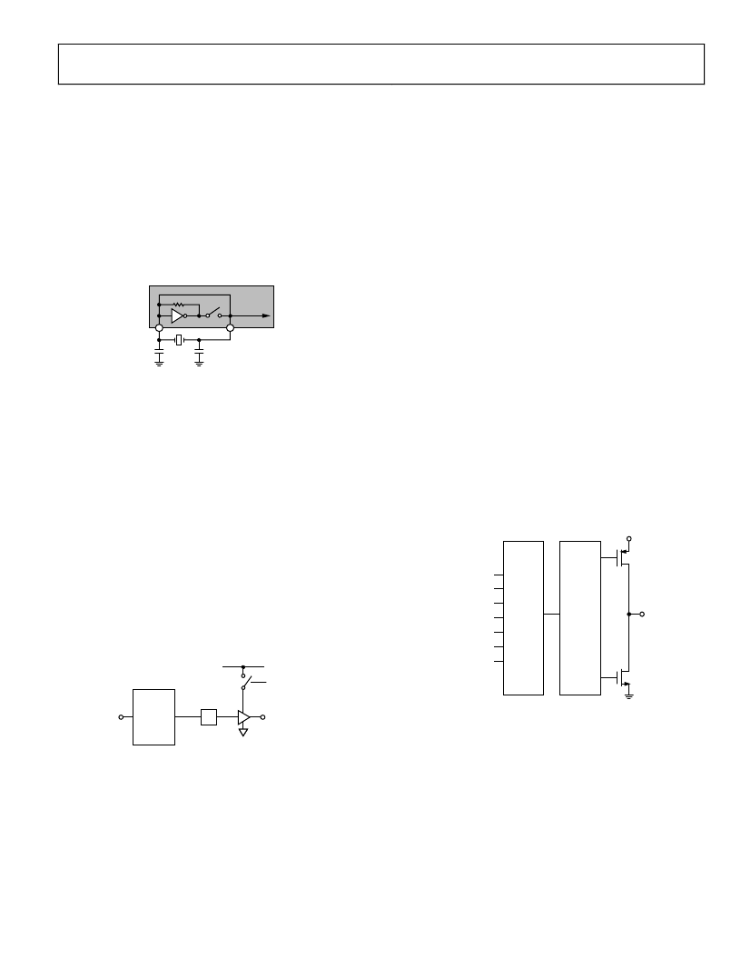
CLKOUT Divider and Buffer
The CLKOUT circuit takes the reference clock signal from the
oscillator section, shown in Figure 5, and supplies a divided-
down 50:50 mark-space signal to the CLKOUT pin. An even
divide from 2 to 30 is available. This divide number is set in
R1_DB(8:11). On power-up, the CLKOUT defaults to
divide-by-8.
DV
DD
CLK
ENABLE BIT
CLK
OUT
OSC1
DIVIDER
1 TO 15
0
÷
2
Figure 6. CLK
OUT
Stage
To disable CLKOUT, set the divide number to 0. The output
buffer can drive up to a 20 pF load with a 10% rise time at
4.8 MHz. Faster edges can result in some spurious feedthrough
to the output. A small series resistor (50 ) can be used to slow
the clock edges to reduce these spurs at F
CLK
.
R Counter
The 3-bit R counter divides the reference input frequency by an
integer from 1 to 7. The divided-down signal is presented as the
reference clock to the phase frequency detector (PFD). The
divide ratio is set in Register 1. Maximizing the PFD frequency
reduces the N value. This reduces the noise multiplied at a rate
of 20 log(N) to the output, as well as reducing occurrences of
spurious components. The R Register defaults to R = 1 on
power-up:
PFD
[Hz] =
XTAL/R
MUXOUT and Lock Detect
The MUXOUT pin allows the user to access various digital
points in the ADF7020. The state of MUXOUT is controlled by
Bits R0_DB(29:31).
Regulator Ready
REGULATOR READY is the default setting on MUXOUT after
the transceiver has been powered up. The power-up time of the
regulator is typically 50 μs. Because the serial interface is
powered from the regulator, the regulator must be at its nominal
voltage before the ADF7020 can be programmed. The status of
the regulator can be monitored at MUXOUT. When the
REGULATOR READY signal on MUXOUT is high,
programming of the ADF7020 can begin.
REGULATOR READY
DIGITAL LOCK DETECT
ANALOG LOCK DETECT
R COUNTER OUTPUT
N COUNTER OUTPUT
PLL TEST MODES
Σ
-
TEST MODES
MUX
CONTROL
DGND
DV
DD
MUXOUT
0
Figure 7. MUXOUT Circuit
Digital Lock Detect
Digital lock detect is active high. The lock detect circuit is
located at the PFD. When the phase error on five consecutive
cycles is less than 15 ns, lock detect is set high. Lock detect
remains high until 25 ns phase error is detected at the PFD.
Because no external components are needed for digital lock
detect, it is more widely used than analog lock detect.
相關(guān)PDF資料 |
PDF描述 |
|---|---|
| ADF7020BCP | High Performance ISM Band FSK/ASK Transceiver IC |
| ADG1204 | 2 pF Off Capacitance, 1 pC Charge Injection, +-15 V/12 V 4:1 iCMOS Multiplexer |
| ADG1204YCP | 2 pF Off Capacitance, 1 pC Charge Injection, +-15 V/12 V 4:1 iCMOS Multiplexer |
| ADG1204YRU | 2 pF Off Capacitance, 1 pC Charge Injection, +-15 V/12 V 4:1 iCMOS Multiplexer |
| ADG202A | Quad SPST Switches(LC2MOS四單刀單擲開關(guān)) |
相關(guān)代理商/技術(shù)參數(shù) |
參數(shù)描述 |
|---|---|
| ADF7020-1 | 制造商:AD 制造商全稱:Analog Devices 功能描述:High Performance FSK/ASK Transceiver IC |
| ADF7020-1BCPZ | 功能描述:IC TX FSK/ASK ISM BAND 48LFCSP RoHS:是 類別:RF/IF 和 RFID >> RF 收發(fā)器 系列:- 產(chǎn)品培訓模塊:Lead (SnPb) Finish for COTS Obsolescence Mitigation Program 標準包裝:30 系列:- 頻率:4.9GHz ~ 5.9GHz 數(shù)據(jù)傳輸率 - 最大:54Mbps 調(diào)制或協(xié)議:* 應用:* 功率 - 輸出:-3dBm 靈敏度:- 電源電壓:2.7 V ~ 3.6 V 電流 - 接收:* 電流 - 傳輸:* 數(shù)據(jù)接口:PCB,表面貼裝 存儲容量:- 天線連接器:PCB,表面貼裝 工作溫度:-25°C ~ 85°C 封裝/外殼:68-TQFN 裸露焊盤 包裝:管件 |
| ADF7020-1BCPZ-RL | 功能描述:IC TX FSK/ASK ISM BAND 48-LFCSP RoHS:是 類別:RF/IF 和 RFID >> RF 收發(fā)器 系列:- 產(chǎn)品培訓模塊:Lead (SnPb) Finish for COTS Obsolescence Mitigation Program 標準包裝:30 系列:- 頻率:4.9GHz ~ 5.9GHz 數(shù)據(jù)傳輸率 - 最大:54Mbps 調(diào)制或協(xié)議:* 應用:* 功率 - 輸出:-3dBm 靈敏度:- 電源電壓:2.7 V ~ 3.6 V 電流 - 接收:* 電流 - 傳輸:* 數(shù)據(jù)接口:PCB,表面貼裝 存儲容量:- 天線連接器:PCB,表面貼裝 工作溫度:-25°C ~ 85°C 封裝/外殼:68-TQFN 裸露焊盤 包裝:管件 |
| ADF7020-1BCPZ-RL7 | 功能描述:IC TX FSK/ASK ISM BAND 48-LFCSP RoHS:是 類別:RF/IF 和 RFID >> RF 收發(fā)器 系列:- 產(chǎn)品培訓模塊:Lead (SnPb) Finish for COTS Obsolescence Mitigation Program 標準包裝:30 系列:- 頻率:4.9GHz ~ 5.9GHz 數(shù)據(jù)傳輸率 - 最大:54Mbps 調(diào)制或協(xié)議:* 應用:* 功率 - 輸出:-3dBm 靈敏度:- 電源電壓:2.7 V ~ 3.6 V 電流 - 接收:* 電流 - 傳輸:* 數(shù)據(jù)接口:PCB,表面貼裝 存儲容量:- 天線連接器:PCB,表面貼裝 工作溫度:-25°C ~ 85°C 封裝/外殼:68-TQFN 裸露焊盤 包裝:管件 |
| ADF7020BCP | 制造商:AD 制造商全稱:Analog Devices 功能描述:High Performance ISM Band FSK/ASK Transceiver IC |
發(fā)布緊急采購,3分鐘左右您將得到回復。