- 您現在的位置:買賣IC網 > PDF目錄373983 > ADF7020 (Analog Devices, Inc.) High Performance ISM Band FSK/ASK Transceiver IC PDF資料下載
參數資料
| 型號: | ADF7020 |
| 廠商: | Analog Devices, Inc. |
| 英文描述: | High Performance ISM Band FSK/ASK Transceiver IC |
| 中文描述: | 高性能ISM頻段FSK信號/賣出收發芯片 |
| 文件頁數: | 9/40頁 |
| 文件大小: | 797K |
| 代理商: | ADF7020 |
第1頁第2頁第3頁第4頁第5頁第6頁第7頁第8頁當前第9頁第10頁第11頁第12頁第13頁第14頁第15頁第16頁第17頁第18頁第19頁第20頁第21頁第22頁第23頁第24頁第25頁第26頁第27頁第28頁第29頁第30頁第31頁第32頁第33頁第34頁第35頁第36頁第37頁第38頁第39頁第40頁
Preliminary Technical Data
ADF7020
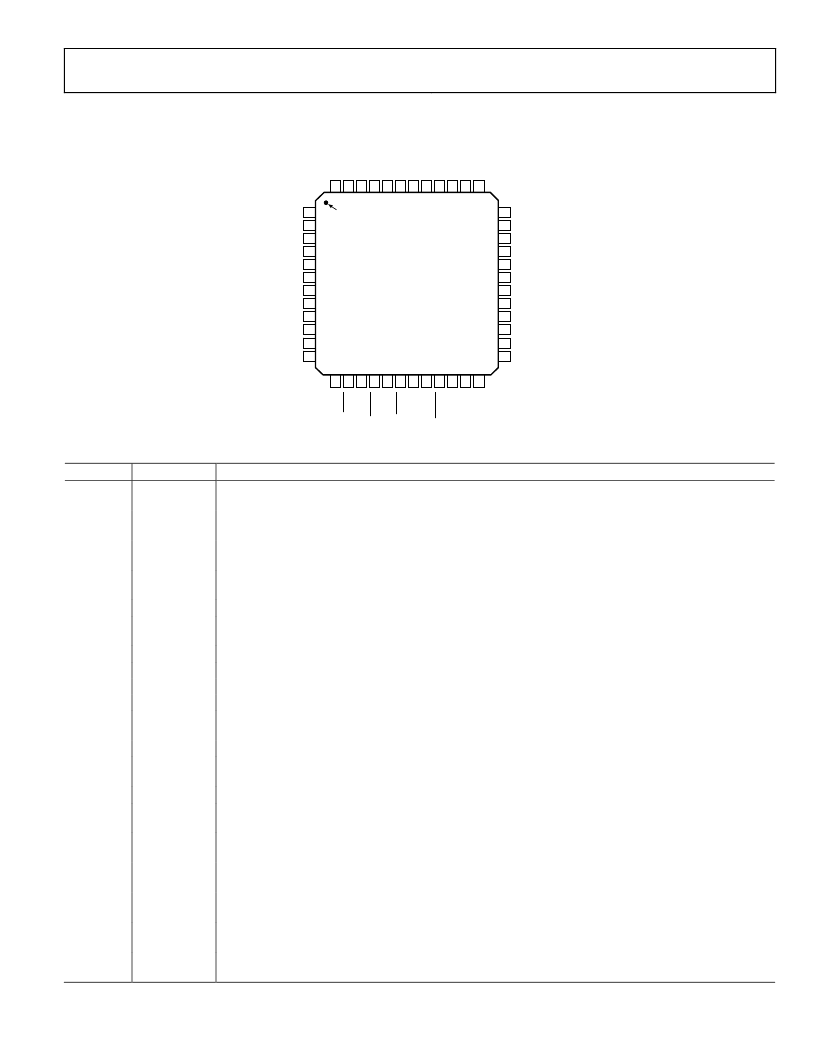
PIN CONFIGURATION AND FUNCTION DESCRIPTIONS
Rev. PrH | Page 9 of 40
36
35
34
33
32
31
30
29
28
27
26
25
4
4
4
4
4
4
4
4
4
3
3
3
1
1
1
1
1
1
1
2
2
2
2
2
ADF7020
TOP VIEW
(Not to Scale)
VCOIN
VREG1
VDD1
RFOUT
RFGND
RFIN
RFINB
R
LNA
VDD4
RSET
VREG4
GND4
M
M
M
M
F
F
G
F
F
G
T
C
CLKOUT
DATA CLK
DATA I/O
INT/LOCK
VDD2
VREG2
ADCIN
GND2
SCLK
SREAD
SDATA
SLE
C
G
G
V
G
V
C
V
V
O
O
M
1
2
3
4
5
6
7
8
9
10
11
12
PIN 1
0
Figure 4. Pin Configuration
Table 4. Pin Function Descriptions
Pin No.
Mnemonic
1
VCOIN
Function
The tuning voltage on this pin determines the output frequency of the voltage controlled oscillator (VCO).
The higher the tuning voltage, the higher the output frequency.
Regulator Voltage for PA Block. A 100 nF capacitor should be placed between this pin and ground for
regulator stability and noise rejection.
Voltage Supply for PA Block. Decoupling capacitors (X7R or Tantalum) of 0.1 μF and 0.01 μF should be placed
as close as possible to this pin.
The modulated signal is available at this pin. Output power levels are from 20 dBm to +13 dBm. The output
should be impedance matched to the desired load using suitable components. See the Transmitter section.
Ground for Output Stage of Transmitter.
LNA Input for Receiver Section. Input matching is required between the antenna and the differential LNA
input to ensure maximum power transfer. See the LNA/PA Matching section.
Complementary LNA Input. See the LNA/PA Matching section.
External bias resistor for LNA. Optimum resistor is 1.1 k with 5% tolerance.
Voltage supply for LNA/MIXER block. This pin should be decoupled to ground with a 0.01 μF capacitor.
External Resistor to Set Charge Pump Current and Some Internal Bias Currents. Use 3.6 k with 5% tolerance.
Regulator Voltage for LNA/MIXER block. A 100 nF capacitor should be placed between this pin and GND for
regulator stability and noise rejection.
Ground for LNA/MIXER block.
Signal Chain Test Pins. These pins are high impedance under normal conditions and should be left
unconnected.
Ground for LNA/MIXER block.
Signal Chain Test Pins. These pins are high impedance under normal conditions and should be left
unconnected.
Chip Enable. Bringing CE low puts the ADF7020 into complete power-down. Register values are lost when CE
is low, and the part must be reprogrammed once CE is brought high.
Load Enable, CMOS Input. When LE goes high, the data stored in the shift registers is loaded into one of the
four latches. A latch is selected using the control bits.
Serial Data Input. The serial data is loaded MSB first with the two LSBs as the control bits. This pin is a high
impedance CMOS input.
Serial Data Output. This pin is used to feed readback data from the ADF7020 to the microcontroller. The SCLK
input is used to clock each readback bit (AFC, ADC readback) from the SREAD pin.
Serial Clock Input. This serial clock is used to clock in the serial data to the registers. The data is latched into
the 24-bit shift register on the CLK rising edge. This pin is a digital CMOS input.
2
VREG1
3
VDD1
4
RFOUT
5
6
RFGND
RFIN
7
8
9
10
11
RFINB
R
LNA
VDD4
RSET
VREG4
12
13–18
GND4
MIX/FILT
19, 22
20, 21, 23
GND4
FILT/TEST_A
24
CE
25
SLE
26
SDATA
27
SREAD
28
SCLK
相關PDF資料 |
PDF描述 |
|---|---|
| ADF7020BCP | High Performance ISM Band FSK/ASK Transceiver IC |
| ADG1204 | 2 pF Off Capacitance, 1 pC Charge Injection, +-15 V/12 V 4:1 iCMOS Multiplexer |
| ADG1204YCP | 2 pF Off Capacitance, 1 pC Charge Injection, +-15 V/12 V 4:1 iCMOS Multiplexer |
| ADG1204YRU | 2 pF Off Capacitance, 1 pC Charge Injection, +-15 V/12 V 4:1 iCMOS Multiplexer |
| ADG202A | Quad SPST Switches(LC2MOS四單刀單擲開關) |
相關代理商/技術參數 |
參數描述 |
|---|---|
| ADF7020-1 | 制造商:AD 制造商全稱:Analog Devices 功能描述:High Performance FSK/ASK Transceiver IC |
| ADF7020-1BCPZ | 功能描述:IC TX FSK/ASK ISM BAND 48LFCSP RoHS:是 類別:RF/IF 和 RFID >> RF 收發器 系列:- 產品培訓模塊:Lead (SnPb) Finish for COTS Obsolescence Mitigation Program 標準包裝:30 系列:- 頻率:4.9GHz ~ 5.9GHz 數據傳輸率 - 最大:54Mbps 調制或協議:* 應用:* 功率 - 輸出:-3dBm 靈敏度:- 電源電壓:2.7 V ~ 3.6 V 電流 - 接收:* 電流 - 傳輸:* 數據接口:PCB,表面貼裝 存儲容量:- 天線連接器:PCB,表面貼裝 工作溫度:-25°C ~ 85°C 封裝/外殼:68-TQFN 裸露焊盤 包裝:管件 |
| ADF7020-1BCPZ-RL | 功能描述:IC TX FSK/ASK ISM BAND 48-LFCSP RoHS:是 類別:RF/IF 和 RFID >> RF 收發器 系列:- 產品培訓模塊:Lead (SnPb) Finish for COTS Obsolescence Mitigation Program 標準包裝:30 系列:- 頻率:4.9GHz ~ 5.9GHz 數據傳輸率 - 最大:54Mbps 調制或協議:* 應用:* 功率 - 輸出:-3dBm 靈敏度:- 電源電壓:2.7 V ~ 3.6 V 電流 - 接收:* 電流 - 傳輸:* 數據接口:PCB,表面貼裝 存儲容量:- 天線連接器:PCB,表面貼裝 工作溫度:-25°C ~ 85°C 封裝/外殼:68-TQFN 裸露焊盤 包裝:管件 |
| ADF7020-1BCPZ-RL7 | 功能描述:IC TX FSK/ASK ISM BAND 48-LFCSP RoHS:是 類別:RF/IF 和 RFID >> RF 收發器 系列:- 產品培訓模塊:Lead (SnPb) Finish for COTS Obsolescence Mitigation Program 標準包裝:30 系列:- 頻率:4.9GHz ~ 5.9GHz 數據傳輸率 - 最大:54Mbps 調制或協議:* 應用:* 功率 - 輸出:-3dBm 靈敏度:- 電源電壓:2.7 V ~ 3.6 V 電流 - 接收:* 電流 - 傳輸:* 數據接口:PCB,表面貼裝 存儲容量:- 天線連接器:PCB,表面貼裝 工作溫度:-25°C ~ 85°C 封裝/外殼:68-TQFN 裸露焊盤 包裝:管件 |
| ADF7020BCP | 制造商:AD 制造商全稱:Analog Devices 功能描述:High Performance ISM Band FSK/ASK Transceiver IC |
發布緊急采購,3分鐘左右您將得到回復。