- 您現(xiàn)在的位置:買賣IC網(wǎng) > PDF目錄373983 > ADF7020 (Analog Devices, Inc.) High Performance ISM Band FSK/ASK Transceiver IC PDF資料下載
參數(shù)資料
| 型號: | ADF7020 |
| 廠商: | Analog Devices, Inc. |
| 英文描述: | High Performance ISM Band FSK/ASK Transceiver IC |
| 中文描述: | 高性能ISM頻段FSK信號/賣出收發(fā)芯片 |
| 文件頁數(shù): | 21/40頁 |
| 文件大小: | 797K |
| 代理商: | ADF7020 |
第1頁第2頁第3頁第4頁第5頁第6頁第7頁第8頁第9頁第10頁第11頁第12頁第13頁第14頁第15頁第16頁第17頁第18頁第19頁第20頁當(dāng)前第21頁第22頁第23頁第24頁第25頁第26頁第27頁第28頁第29頁第30頁第31頁第32頁第33頁第34頁第35頁第36頁第37頁第38頁第39頁第40頁
Preliminary Technical Data
ADF7020
APPLICATIONS SECTION
LNA/PA MATCHING
The ADF7020 exhibits optimum performance in terms of
sensitivity, transmit power, and current consumption only if its
RF input and output ports are properly matched to the antenna
impedance. For cost-sensitive applications, the ADF7020 is
equipped with an internal Rx/Tx switch, which facilitates the
use of a simple combined passive PA/LNA matching network.
Alternatively, an external Rx/Tx switch such as the Analog
Devices ADG919 can be used, which yields a slightly improved
receiver sensitivity and lower transmitter power consumption.
External Rx/Tx Switch
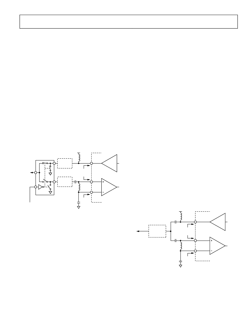
Figure 18 shows a configuration using an external Rx/Tx switch.
This configuration allows an independent optimization of the
matching and filter network in the transmit and receive path,
and is, therefore, more flexible and less difficult to design than
the configuration using the internal Rx/Tx switch. The PA is
biased through inductor L1, while C1 blocks dc current. Both
elements, L1 and C1, also form the matching network, which
transforms the source impedance into the optimum PA load
impedance, Z
OPT
_PA.
Rev. PrH | Page 21 of 40
0
PA
LNA
PA_OUT
RFIN
RFINB
V
BAT
L1
ADF7020
ADG919
OPTIONAL
BPF
(SAW)
OPTIONAL
LPF
L
A
C
A
C
B
Z
IN
_RFIN
Z
OPT
_PA
Z
IN
_RFIN
ANTENNA
Rx/Tx – SELECT
Figure 18. ADF7020 with External Rx/Tx Switch
Z
OPT
_PA depends on various factors such as the required output
power, the frequency range, the supply voltage range, and the
temperature range. Selecting an appropriate Z
OPT
_PA helps to
minimize the Tx current consumption in the application. This
datasheet contains a number of Z
OPT
_PA values for representa-
tive conditions. Under certain conditions, however, it is
recommended to obtain a suitable Z
OPT
_PA value by means of a
load-pull measurement.
Due to the differential LNA input, the LNA matching network
must be designed to provide both a single-ended to differential
conversion and a complex conjugate impedance match. The
network with the lowest component count that can satisfy these
requirements is the configuration shown in Figure 18, which
consists of two capacitors and one inductor. A first-order
implementation of the matching network can be obtained by
understanding the arrangement as two L-type matching
networks in a back-to-back configuration. Due to the
asymmetry of the network with respect to ground, a compro-
mise between the input reflection coefficient and the maximum
differential signal swing at the LNA input must be established.
The use of appropriate CAD software is strongly recommended
for this optimization.
Depending on the antenna configuration, the user might need a
harmonic filter at the PA output to satisfy the spurious emission
requirement of the applicable government regulations. The
harmonic filter can be implemented in various ways, such as a
discrete LC-filter. Dielectric low-pass filter components such as
the LFL18924MTC1A052 (for operation in the 915 MHz band),
or LFL18869MTC2A160 (for operation in the 868 MHz band),
both by Murata Mfg. Co., Ltd., represent an attractive alternative
to discrete designs. The immunity of the ADF7020 to strong
out-of-band interference can be improved by adding a band-
pass filter in the Rx path. Apart from discrete designs, SAW or
dielectric filter components such as the
SAFCH869MAM0T00B0S, SAFCH915MAL0N00B0S,
DCFB2869MLEJAA-TT1, or DCFB3915MLDJAA-TT1, all by
Murata Mfg. Co., Ltd., are well suited for this purpose.
Internal Rx/Tx Switch
Figure 19 shows the ADF7020 in a configuration where the
internal Rx/Tx switch is used with a combined LNA/PA
matching network. Depending on the application, the slight
performance degradation caused by the internal Rx/Tx switch
might be acceptable, allowing the user to take advantage of the
cost-saving potential of this solution. The design of the
combined matching network must compensate for the
reactance presented by the networks in the Tx and the Rx paths,
taking the state of the Rx/Tx switch into consideration.
0
PA
LNA
PA_OUT
RFIN
RFINB
V
BAT
L1
ADF7020
OPTIONAL
BPF OR LPF
L
A
C
A
C1
C
B
Z
IN
_RFIN
Z
OPT
_PA
Z
IN
_RFIN
ANTENNA
Figure 19. ADF7020 with Internal Rx/Tx Switch
The procedure typically requires several iterations until an
acceptable compromise has been reached. The successful
implementation of a combined LNA/PA matching network for
the ADF7020 is critically dependent on the availability of an
相關(guān)PDF資料 |
PDF描述 |
|---|---|
| ADF7020BCP | High Performance ISM Band FSK/ASK Transceiver IC |
| ADG1204 | 2 pF Off Capacitance, 1 pC Charge Injection, +-15 V/12 V 4:1 iCMOS Multiplexer |
| ADG1204YCP | 2 pF Off Capacitance, 1 pC Charge Injection, +-15 V/12 V 4:1 iCMOS Multiplexer |
| ADG1204YRU | 2 pF Off Capacitance, 1 pC Charge Injection, +-15 V/12 V 4:1 iCMOS Multiplexer |
| ADG202A | Quad SPST Switches(LC2MOS四單刀單擲開關(guān)) |
相關(guān)代理商/技術(shù)參數(shù) |
參數(shù)描述 |
|---|---|
| ADF7020-1 | 制造商:AD 制造商全稱:Analog Devices 功能描述:High Performance FSK/ASK Transceiver IC |
| ADF7020-1BCPZ | 功能描述:IC TX FSK/ASK ISM BAND 48LFCSP RoHS:是 類別:RF/IF 和 RFID >> RF 收發(fā)器 系列:- 產(chǎn)品培訓(xùn)模塊:Lead (SnPb) Finish for COTS Obsolescence Mitigation Program 標(biāo)準(zhǔn)包裝:30 系列:- 頻率:4.9GHz ~ 5.9GHz 數(shù)據(jù)傳輸率 - 最大:54Mbps 調(diào)制或協(xié)議:* 應(yīng)用:* 功率 - 輸出:-3dBm 靈敏度:- 電源電壓:2.7 V ~ 3.6 V 電流 - 接收:* 電流 - 傳輸:* 數(shù)據(jù)接口:PCB,表面貼裝 存儲容量:- 天線連接器:PCB,表面貼裝 工作溫度:-25°C ~ 85°C 封裝/外殼:68-TQFN 裸露焊盤 包裝:管件 |
| ADF7020-1BCPZ-RL | 功能描述:IC TX FSK/ASK ISM BAND 48-LFCSP RoHS:是 類別:RF/IF 和 RFID >> RF 收發(fā)器 系列:- 產(chǎn)品培訓(xùn)模塊:Lead (SnPb) Finish for COTS Obsolescence Mitigation Program 標(biāo)準(zhǔn)包裝:30 系列:- 頻率:4.9GHz ~ 5.9GHz 數(shù)據(jù)傳輸率 - 最大:54Mbps 調(diào)制或協(xié)議:* 應(yīng)用:* 功率 - 輸出:-3dBm 靈敏度:- 電源電壓:2.7 V ~ 3.6 V 電流 - 接收:* 電流 - 傳輸:* 數(shù)據(jù)接口:PCB,表面貼裝 存儲容量:- 天線連接器:PCB,表面貼裝 工作溫度:-25°C ~ 85°C 封裝/外殼:68-TQFN 裸露焊盤 包裝:管件 |
| ADF7020-1BCPZ-RL7 | 功能描述:IC TX FSK/ASK ISM BAND 48-LFCSP RoHS:是 類別:RF/IF 和 RFID >> RF 收發(fā)器 系列:- 產(chǎn)品培訓(xùn)模塊:Lead (SnPb) Finish for COTS Obsolescence Mitigation Program 標(biāo)準(zhǔn)包裝:30 系列:- 頻率:4.9GHz ~ 5.9GHz 數(shù)據(jù)傳輸率 - 最大:54Mbps 調(diào)制或協(xié)議:* 應(yīng)用:* 功率 - 輸出:-3dBm 靈敏度:- 電源電壓:2.7 V ~ 3.6 V 電流 - 接收:* 電流 - 傳輸:* 數(shù)據(jù)接口:PCB,表面貼裝 存儲容量:- 天線連接器:PCB,表面貼裝 工作溫度:-25°C ~ 85°C 封裝/外殼:68-TQFN 裸露焊盤 包裝:管件 |
| ADF7020BCP | 制造商:AD 制造商全稱:Analog Devices 功能描述:High Performance ISM Band FSK/ASK Transceiver IC |
發(fā)布緊急采購,3分鐘左右您將得到回復(fù)。