- 您現(xiàn)在的位置:買賣IC網(wǎng) > PDF目錄374032 > ADSP-21061L (Analog Devices, Inc.) ADSP-2106x SHARC DSP Microcomputer Family PDF資料下載
參數(shù)資料
| 型號(hào): | ADSP-21061L |
| 廠商: | Analog Devices, Inc. |
| 英文描述: | ADSP-2106x SHARC DSP Microcomputer Family |
| 中文描述: | 的ADSP - 2106x SHARC處理器DSP的微機(jī)家庭 |
| 文件頁(yè)數(shù): | 4/47頁(yè) |
| 文件大小: | 367K |
| 代理商: | ADSP-21061L |
第1頁(yè)第2頁(yè)第3頁(yè)當(dāng)前第4頁(yè)第5頁(yè)第6頁(yè)第7頁(yè)第8頁(yè)第9頁(yè)第10頁(yè)第11頁(yè)第12頁(yè)第13頁(yè)第14頁(yè)第15頁(yè)第16頁(yè)第17頁(yè)第18頁(yè)第19頁(yè)第20頁(yè)第21頁(yè)第22頁(yè)第23頁(yè)第24頁(yè)第25頁(yè)第26頁(yè)第27頁(yè)第28頁(yè)第29頁(yè)第30頁(yè)第31頁(yè)第32頁(yè)第33頁(yè)第34頁(yè)第35頁(yè)第36頁(yè)第37頁(yè)第38頁(yè)第39頁(yè)第40頁(yè)第41頁(yè)第42頁(yè)第43頁(yè)第44頁(yè)第45頁(yè)第46頁(yè)第47頁(yè)
–4–
ADSP-21061/ADSP-21061L
REV. B
ADSP-21000 FAMILY CORE ARCHITECTURE
The ADSP-21061 includes the following architectural features
of the ADSP-21000 family core. The ADSP-21061 is code and
function compatible with the ADSP-21060/ADSP-21062 and
the ADSP-21020.
Independent, Parallel Computation Units
The arithmetic/logic unit (ALU), multiplier and shifter all per-
form single-cycle instructions. The three units are arranged in
parallel, maximizing computational throughput. Single multi-
function instructions execute parallel ALU and multiplier op-
erations. These computation units support IEEE 32-bit single-
precision floating-point, extended precision 40-bit floating-
point and 32-bit fixed-point data formats.
3
4
RESET
JTAG
7
ADSP-21061/
ADSP-21061L
BMS
ADDR
31-0
DATA
47-0
C
A
D
SERIAL
DEVICE
(OPTIONAL)
SERIAL
DEVICE
(OPTIONAL)
CS
ADDR
DATA
BOOT
EPROM
(OPTIONAL)
ADDR
ACK
CS
MEMORY
AND
PERIPHERALS
(OPTIONAL)
OE
WE
DATA
DMA DEVICE
(OPTIONAL)
DATA
ADDR
DATA
HOST
PROCESSOR
INTERFACE
(OPTIONAL)
1x CLOCK
CS
HBR
HBG
REDY
RD
WR
ACK
MS
3-0
PAGE
SBTS
SW
ADRCLK
BR
1-6
CPA
DMAR
1-2
DMAG
1-2
CLKIN
EBOOT
LBOOT
IRQ
2-0
FLAG
3-0
TIMEXP
TCLK0
RCLK0
TFS0
RSF0
DT0
DR0
TCLK1
RCLK1
TFS1
RSF1
DT1
DR1
RPBA
ID
2-0
TO GND
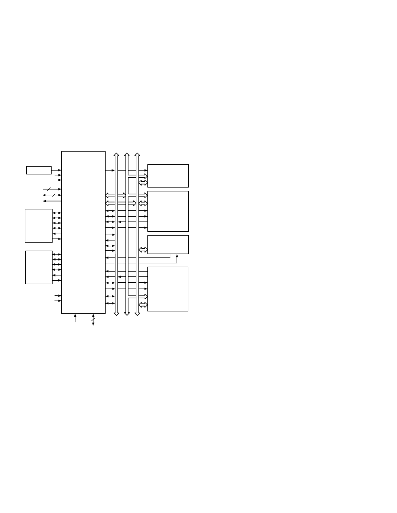
Figure 2. ADSP-21061/ADSP-21061L System
Data Register File
A general purpose data register file is used for transferring data
between the computation units and the data buses, and for
storing intermediate results. This 10-port, 32-register (16 pri-
mary, 16 secondary) register file, combined with the ADSP-
21000 Harvard architecture, allows unconstrained data flow
between computation units and internal memory.
Single-Cycle Fetch of Instruction and Two Operands
The ADSP-21061 features an enhanced Harvard architecture in
which the data memory (DM) bus transfers data and the pro-
gram memory (PM) bus transfers both instructions and data
(see Figure 1). With its separate program and data memory
buses and on-chip instruction cache, the processor can simulta-
neously fetch two operands and an instruction (from the cache),
all in a single cycle.
Instruction Cache
The ADSP-21061 includes an on-chip instruction cache that
enables three-bus operation for fetching an instruction and two
data values. The cache is selective—only the instructions whose
fetches conflict with PM bus data accesses are cached. This
allows full-speed execution of core, looped operations such as
digital filter multiply-accumulates and FFT butterfly processing.
Data Address Generators with Hardware Circular Buffers
The ADSP-21061’s two data address generators (DAGs) imple-
ment circular data buffers in hardware. Circular buffers allow
efficient programming of delay lines and other data structures
required in digital signal processing, and are commonly used in
digital filters and Fourier transforms. The ADSP-21061 two
DAGs contain sufficient registers to allow the creation of up to
32 circular buffers (16 primary register sets, 16 secondary). The
DAGs automatically handle address pointer wraparound, reduc-
ing overhead, increasing performance and simplifying imple-
mentation. Circular buffers can start and end at any memory
location.
Flexible Instruction Set
The 48-bit instruction word accommodates a variety of parallel
operations, for concise programming. For example, the ADSP-
21061 can conditionally execute a multiply, an add, a subtract
and a branch, all in a single instruction.
ADSP-21061 FEATURES
Augmenting the ADSP-21000 family core, the ADSP-21061
adds the following architectural features:
Dual-Ported On-Chip Memory
The ADSP-21061 contains 1 megabit of on-chip SRAM, orga-
nized as two banks of 0.5 Mbits each. Each bank has eight 16-
bit columns with 4K 16-bit words per column. Each memory
block is dual-ported for single-cycle, independent accesses by
the core processor and I/O processor or DMA controller. The
dual-ported memory and separate on-chip buses allow two data
transfers from the core and one from I/O, all in a single cycle
(see Figure 4 for the ADSP-21061 Memory Map).
On the ADSP-21061, the memory can be configured as a maxi-
mum of 32K words of 32-bit data, 64K words for 16-bit data,
16K words of 48-bit instructions (and 40-bit data) or combina-
tions of different word sizes up to 1 megabit. All the memory
can be accessed as 16-bit, 32-bit or 48-bit.
A 16-bit floating-point storage format is supported that effec-
tively doubles the amount of data that may be stored on chip.
Conversion between the 32-bit floating-point and 16-bit floating-
point formats is done in a single instruction.
While each memory block can store combinations of code and
data, accesses are most efficient when one block stores data,
using the DM bus for transfers, and the other block stores in-
structions and data, using the PM bus for transfers. Using the
DM and PM buses in this way, with one dedicated to each
memory block, assures single-cycle execution with two data
transfers. In this case, the instruction must be available in the
cache. Single-cycle execution is also maintained when one of the
data operands is transferred to or from off-chip, via the ADSP-
21061’s external port.
相關(guān)PDF資料 |
PDF描述 |
|---|---|
| ADSP-21061LAS-160 | ADSP-2106x SHARC DSP Microcomputer Family |
| ADSP-21061LAS-176 | ADSP-2106x SHARC DSP Microcomputer Family |
| ADSP-21061KS-160 | ADSP-2106x SHARC DSP Microcomputer Family |
| ADSP-21061KS-200 | ADSP-2106x SHARC DSP Microcomputer Family |
| ADSP-21061LKB-160 | ADSP-2106x SHARC DSP Microcomputer Family |
相關(guān)代理商/技術(shù)參數(shù) |
參數(shù)描述 |
|---|---|
| ADSP-21061LAS-160 | 制造商:AD 制造商全稱:Analog Devices 功能描述:ADSP-2106x SHARC DSP Microcomputer Family |
| ADSP-21061LAS-176 | 制造商:Analog Devices 功能描述:DSP Floating-Point 32-Bit 44MHz 44MIPS 240-Pin MQFP Tray 制造商:Analog Devices 功能描述:IC MICROCOMPUTER DSP |
| ADSP-21061LASZ-176 | 功能描述:IC DSP CONTROLLER 32BIT 240MQFP RoHS:是 類別:集成電路 (IC) >> 嵌入式 - DSP(數(shù)字式信號(hào)處理器) 系列:SHARC® 標(biāo)準(zhǔn)包裝:40 系列:TMS320DM64x, DaVinci™ 類型:定點(diǎn) 接口:I²C,McASP,McBSP 時(shí)鐘速率:400MHz 非易失內(nèi)存:外部 芯片上RAM:160kB 電壓 - 輸入/輸出:3.30V 電壓 - 核心:1.20V 工作溫度:0°C ~ 90°C 安裝類型:表面貼裝 封裝/外殼:548-BBGA,F(xiàn)CBGA 供應(yīng)商設(shè)備封裝:548-FCBGA(27x27) 包裝:托盤 配用:TMDSDMK642-0E-ND - DEVELPER KIT W/NTSC CAMERA296-23038-ND - DSP STARTER KIT FOR TMS320C6416296-23059-ND - FLASHBURN PORTING KIT296-23058-ND - EVAL MODULE FOR DM642TMDSDMK642-ND - DEVELOPER KIT W/NTSC CAMERA |
| ADSP-21061LKB-160 | 功能描述:IC DSP CONTROLLER 32BIT 225BGA RoHS:否 類別:集成電路 (IC) >> 嵌入式 - DSP(數(shù)字式信號(hào)處理器) 系列:SHARC® 標(biāo)準(zhǔn)包裝:2 系列:StarCore 類型:SC140 內(nèi)核 接口:DSI,以太網(wǎng),RS-232 時(shí)鐘速率:400MHz 非易失內(nèi)存:外部 芯片上RAM:1.436MB 電壓 - 輸入/輸出:3.30V 電壓 - 核心:1.20V 工作溫度:-40°C ~ 105°C 安裝類型:表面貼裝 封裝/外殼:431-BFBGA,F(xiàn)CBGA 供應(yīng)商設(shè)備封裝:431-FCPBGA(20x20) 包裝:托盤 |
| ADSP-21061LKB-176 | 制造商:AD 制造商全稱:Analog Devices 功能描述:DSP Microcomputer Family |
發(fā)布緊急采購(gòu),3分鐘左右您將得到回復(fù)。