- 您現(xiàn)在的位置:買賣IC網(wǎng) > PDF目錄374039 > ADUC836BS (ANALOG DEVICES INC) MicroConverter, Dual 16-Bit-ADCs with Embedded 62 kB Flash MCU PDF資料下載
參數(shù)資料
| 型號: | ADUC836BS |
| 廠商: | ANALOG DEVICES INC |
| 元件分類: | 微控制器/微處理器 |
| 英文描述: | MicroConverter, Dual 16-Bit-ADCs with Embedded 62 kB Flash MCU |
| 中文描述: | 8-BIT, FLASH, 12.58 MHz, MICROCONTROLLER, PQFP52 |
| 封裝: | 14 X 14 MM, MO-022-AC-1, MQFP-52 |
| 文件頁數(shù): | 34/80頁 |
| 文件大小: | 5913K |
| 代理商: | ADUC836BS |
第1頁第2頁第3頁第4頁第5頁第6頁第7頁第8頁第9頁第10頁第11頁第12頁第13頁第14頁第15頁第16頁第17頁第18頁第19頁第20頁第21頁第22頁第23頁第24頁第25頁第26頁第27頁第28頁第29頁第30頁第31頁第32頁第33頁當前第34頁第35頁第36頁第37頁第38頁第39頁第40頁第41頁第42頁第43頁第44頁第45頁第46頁第47頁第48頁第49頁第50頁第51頁第52頁第53頁第54頁第55頁第56頁第57頁第58頁第59頁第60頁第61頁第62頁第63頁第64頁第65頁第66頁第67頁第68頁第69頁第70頁第71頁第72頁第73頁第74頁第75頁第76頁第77頁第78頁第79頁第80頁
ADuC836
–34–
programmed to appear at Pin 3 or Pin 12. It should be noted
that in 12-bit mode, the DAC voltage output will be updated
as soon as the DACL data SFR has been written; therefore, the
DAC data registers should be updated as DACH first, followed
by DACL. The 12-bit DAC data should be written into DACH/L
right-justified such that DACL contains the lower eight bits, and
the lower nibble of DACH contains the upper four bits.
Table XV. DACCON SFR Bit Designations
Bit Name Description
7 ––– Reserved for Future Use
6 ––– Reserved for Future Use
5 ––– Reserved for Future Use
4 DACPIN DAC Output Pin Select.
Set by user to direct the DAC output to Pin 12 (P1.7/AIN4/DAC).
Cleared by user to direct the DAC output to Pin 3 (P1.2/DAC/IEXC1).
3 DAC8 DAC 8-bit Mode Bit.
Set by user to enable 8-bit DAC operation. In this mode, the 8 bits in DACL SFR are routed to the 8 MSBs
of the DAC, and the 4 LSBs of the DAC are set to zero.
Cleared by user to operate the DAC in its normal 12-bit mode of operation.
2 DACRN DAC Output Range Bit.
Set by user to configure DAC range of 0 to AV
DD
.
Cleared by user to configure DAC range of 0 V to 2.5 V (V
REF
).
1
DACCLR
DAC Clear Bit.
Set to 1 by user to enable normal DAC operation.
Cleared to 0 by user to reset DAC data registers DACL/H to zero.
0 DACEN DAC Enable Bit.
Set to 1 by user to enable normal DAC operation.
Cleared to 0 by user to power down the DAC.
DACH/L DAC Data Registers
Function DAC Data Registers, written by user to update the DAC output.
SFR Address DACL (DAC Data Low Byte)
DACH (DAC Data High Byte)
Power-On Default Value 00H
Bit Addressable No
FBH
FCH
Both Registers
Both Registers
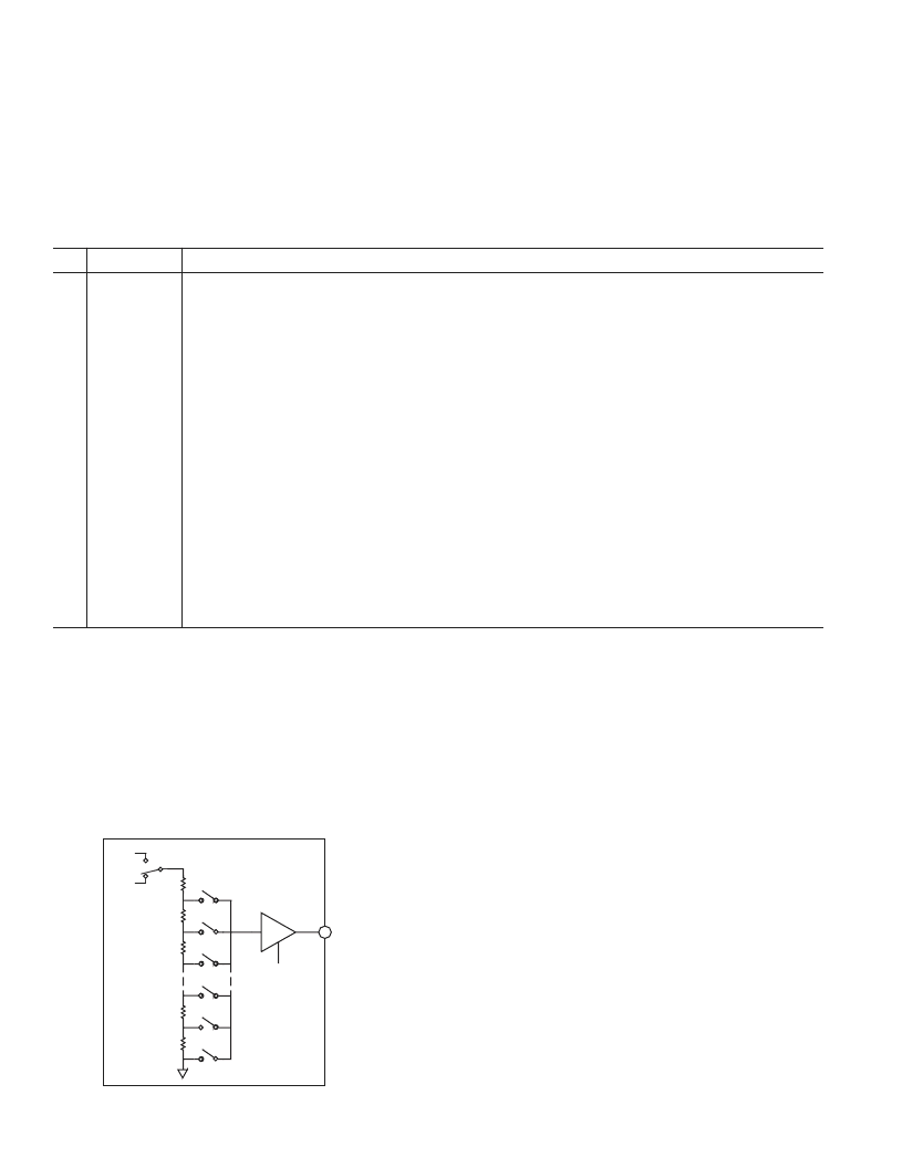
Using the D/A Converter
The on-chip D/A converter architecture consists of a resistor
string DAC followed by an output buffer amplifier, the functional
equivalent of which is illustrated in Figure 21.
R
R
R
R
R
ADuC836
AV
DD
V
REF
OUTPUT
BUFFER
DAC
12
HIGH-Z
DISABLE
(FROM MCU)
Figure 21. Resistor String DAC Functional Equivalent
Features of this architecture include inherent guaranteed monoto-
nicity and excellent differential linearity. As illustrated in Figure 21,
the reference source for the DAC is user selectable in software. It
can be either AV
DD
or V
REF
. In 0-to-AV
DD
mode, the DAC output
transfer function spans from 0 V to the voltage at the AV
DD
pin.
In 0-to-V
REF
mode, the DAC output transfer function spans from
0 V to the internal V
REF
(2.5 V). The DAC output buffer amplifier
features a true rail-to-rail output stage implementation. This means
that, unloaded, each output is capable of swinging to within less than
100 mV of both AV
DD
and ground. Moreover, the DAC’s linear-
ity specification (when driving a 10 k
resistive load to ground)
is guaranteed through the full transfer function except codes 0
to 48 in 0-to-V
REF
mode and 0 to 100 and 3950 to 4095 in 0-to-
V
DD
mode.
Linearity degradation near ground and V
DD
is caused by saturation
of the output amplifier, and a general representation of its effects
(neglecting offset and gain error) is illustrated in Figure 22. The
dotted line in Figure 22 indicates the ideal transfer function, and
the solid line represents what the transfer function might look
like with endpoint nonlinearities due to saturation of the output
amplifier.
DAC
The ADuC836 incorporates a 12-bit voltage output DAC
on-chip. It has a rail-to-rail voltage output buffer capable of driving
10 k
/100 pF. It has two selectable ranges, 0 V to V
REF
(the inter-
nal band gap 2.5 V reference) and 0 V to AV
DD
. It can operate
in 12-bit or 8-bit mode. The DAC has a control register, DACCON,
and two data registers, DACH/L. The DAC output can be
REV. A
相關(guān)PDF資料 |
PDF描述 |
|---|---|
| ADUC842BCP62-3 | MicroConverter 12-Bit ADCs and DACs with Embedded High Speed 62-kB Flash MCU |
| ADUC843BCP62-5 | MicroConverter 12-Bit ADCs and DACs with Embedded High Speed 62-kB Flash MCU |
| ADUC842BCP62-5 | MicroConverter 12-Bit ADCs and DACs with Embedded High Speed 62-kB Flash MCU |
| ADUC843BCP62-3 | MicroConverter 12-Bit ADCs and DACs with Embedded High Speed 62-kB Flash MCU |
| ADUC842BCP32-3 | MicroConverter 12-Bit ADCs and DACs with Embedded High Speed 62-kB Flash MCU |
相關(guān)代理商/技術(shù)參數(shù) |
參數(shù)描述 |
|---|---|
| ADUC836BS | 制造商:Analog Devices 功能描述:IC SEMICONDUCTOR ((NS)) |
| ADUC836BSZ | 功能描述:IC ADC DUAL 16BIT W/MCU 52-MQFP RoHS:是 類別:集成電路 (IC) >> 嵌入式 - 微控制器, 系列:MicroConverter® ADuC8xx 標準包裝:250 系列:56F8xxx 核心處理器:56800E 芯體尺寸:16-位 速度:60MHz 連通性:CAN,SCI,SPI 外圍設(shè)備:POR,PWM,溫度傳感器,WDT 輸入/輸出數(shù):21 程序存儲器容量:40KB(20K x 16) 程序存儲器類型:閃存 EEPROM 大小:- RAM 容量:6K x 16 電壓 - 電源 (Vcc/Vdd):2.25 V ~ 3.6 V 數(shù)據(jù)轉(zhuǎn)換器:A/D 6x12b 振蕩器型:內(nèi)部 工作溫度:-40°C ~ 125°C 封裝/外殼:48-LQFP 包裝:托盤 配用:MC56F8323EVME-ND - BOARD EVALUATION MC56F8323 |
| ADUC841 | 制造商:AD 制造商全稱:Analog Devices 功能描述:MicroConverter 12-Bit ADCs and DACs with Embedded High Speed 62-kB Flash MCU |
| ADUC841BCP32-5 | 制造商:Analog Devices 功能描述:MICROCONVERTER 1-CYCLE VERSION ADUC829 - Trays |
| ADUC841BCP62-3 | 制造商:Analog Devices 功能描述:MCU 8-Bit ADuC8xx 8052 CISC 62KB Flash 3V 56-Pin LFCSP EP 制造商:Rochester Electronics LLC 功能描述:8BIT CISC 62KB FLASH 20MHZ 3.3V 56LFCSP - Bulk |
發(fā)布緊急采購,3分鐘左右您將得到回復。