- 您現在的位置:買賣IC網 > PDF目錄374039 > ADUC836BS (ANALOG DEVICES INC) MicroConverter, Dual 16-Bit-ADCs with Embedded 62 kB Flash MCU PDF資料下載
參數資料
| 型號: | ADUC836BS |
| 廠商: | ANALOG DEVICES INC |
| 元件分類: | 微控制器/微處理器 |
| 英文描述: | MicroConverter, Dual 16-Bit-ADCs with Embedded 62 kB Flash MCU |
| 中文描述: | 8-BIT, FLASH, 12.58 MHz, MICROCONTROLLER, PQFP52 |
| 封裝: | 14 X 14 MM, MO-022-AC-1, MQFP-52 |
| 文件頁數: | 57/80頁 |
| 文件大小: | 5913K |
| 代理商: | ADUC836BS |
第1頁第2頁第3頁第4頁第5頁第6頁第7頁第8頁第9頁第10頁第11頁第12頁第13頁第14頁第15頁第16頁第17頁第18頁第19頁第20頁第21頁第22頁第23頁第24頁第25頁第26頁第27頁第28頁第29頁第30頁第31頁第32頁第33頁第34頁第35頁第36頁第37頁第38頁第39頁第40頁第41頁第42頁第43頁第44頁第45頁第46頁第47頁第48頁第49頁第50頁第51頁第52頁第53頁第54頁第55頁第56頁當前第57頁第58頁第59頁第60頁第61頁第62頁第63頁第64頁第65頁第66頁第67頁第68頁第69頁第70頁第71頁第72頁第73頁第74頁第75頁第76頁第77頁第78頁第79頁第80頁
ADuC836
–57–
SCON UART Serial Port Control Registers
SFR Address 98H
Power-On Default Value 00H
Bit Addressable Yes
Table XXX. SCON SFR Bit Designations
Bit Name Description
7 SM0 UART Serial Mode Select Bits.
6 SM1 These bits select the Serial Port operating mode as follows:
SM0
SM1
0
0
0
1
1
0
1
1
5 SM2 Multiprocessor Communication Enable Bit.
Enables multiprocessor communication in Modes 2 and 3. In Mode 0, SM2 should be cleared. In Mode 1, if
SM2 is set, RI will not be activated if a valid stop bit was not received. If SM2 is cleared, RI will be set as soon
as the byte of data has been received. In Modes 2 or 3, if SM2 is set, RI will not be activated if the received ninth
data bit in RB8 is 0. If SM2 is cleared, RI will be set as soon as the byte of data has been received.
4 REN Serial Port Receive Enable Bit.
Set by user software to enable serial port reception.
Cleared by user software to disable serial port reception.
3 TB8 Serial Port Transmit (Bit 9).
The data loaded into TB8 will be the ninth data bit that will be transmitted in Modes 2 and 3.
2 RB8 Serial Port Receiver Bit 9.
The ninth data bit received in Modes 2 and 3 is latched into RB8. For Mode 1, the stop bit is latched into RB8.
1 TI Serial Port Transmit Interrupt Flag.
Set by hardware at the end of the eighth bit in Mode 0, or at the beginning of the stop bit in Modes 1, 2, and 3.
TI must be cleared by user software.
0 RI Serial Port Receive Interrupt Flag.
Set by hardware at the end of the eighth bit in Mode 0, or halfway through the stop bit in Modes 1, 2, and 3.
RI must be cleared by software.
Selected Operating Mode
Mode 0: Shift Register, fixed baud rate (f
CORE
/12)
Mode 1: 8-bit UART, variable baud rate
Mode 2: 9-bit UART, fixed baud rate (f
CORE
/64) or (f
CORE
/32)
Mode 3: 9-bit UART, variable baud rate
UART SERIAL INTERFACE
The serial port is full-duplex, meaning it can transmit and receive
simultaneously. It is also receive-buffered, meaning it can com-
mence reception of a second byte before a previously received byte
has been read from the receive register. However, if the first byte
still has not been read by the time reception of the second byte is
complete, the first byte will be lost. The physical interface to the
serial data network is via pins RxD(P3.0) and TxD(P3.1), while
the SFR interface to the UART comprises the following registers:
SBUF
The serial port receive and transmit registers are both accessed
through the SBUF SFR (SFR address = 99H). Writing to SBUF
loads the transmit register, and reading SBUF accesses a physi-
cally separate receive register.
UART OPERATING MODES
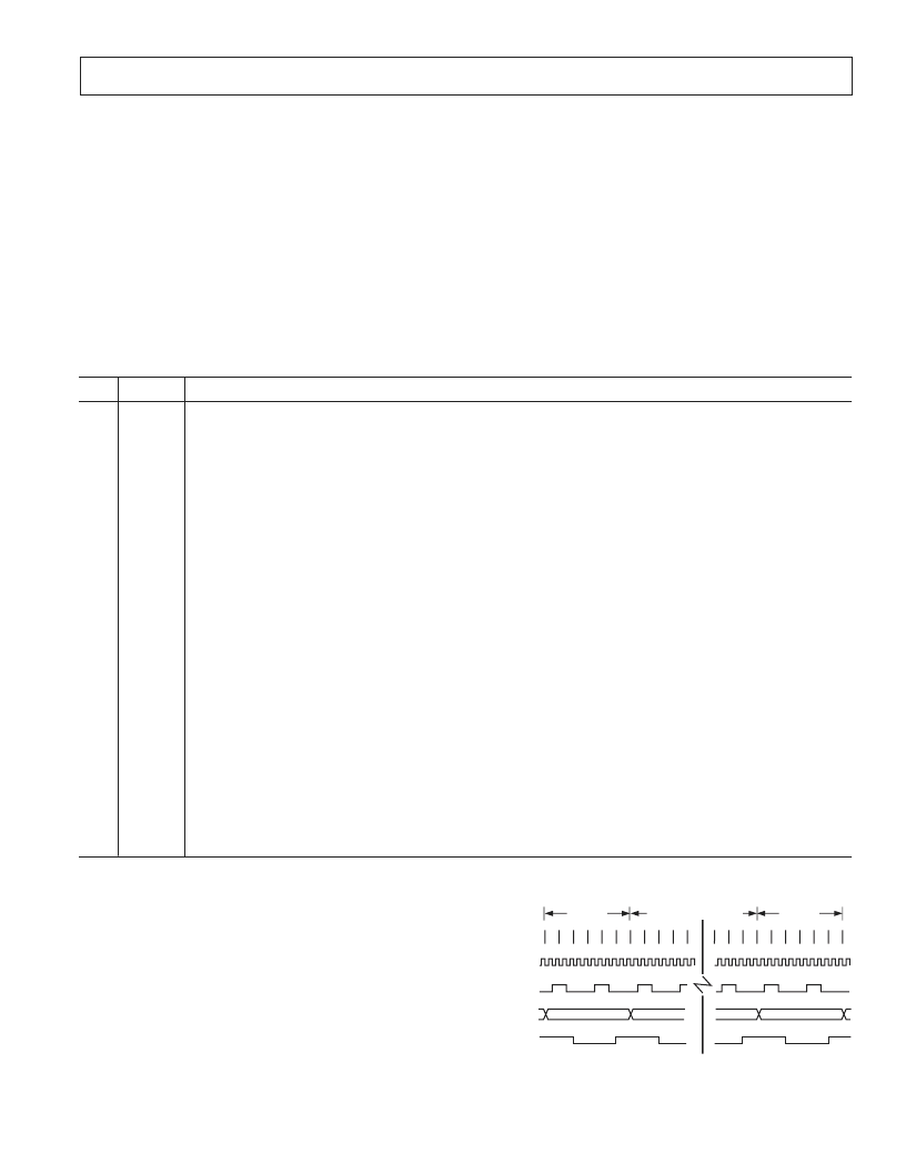
Mode 0: 8-Bit Shift Register Mode
Mode 0 is selected by clearing both the SM0 and SM1 bits in
the SFR SCON. Serial data enters and exits through RxD. TxD
outputs the shift clock. Eight data bits are transmitted or received.
Transmission is initiated by any instruction that writes to SBUF.
The data is shifted out of the RxD line. The 8 bits are transmitted
with the least significant bit (LSB) first, as shown in Figure 54.
Reception is initiated when the Receive Enable bit (REN) is 1 and
the Receive Interrupt bit (RI) is 0. When RI is cleared, the data
is clocked into the RxD line and the clock pulses are output from
the TxD line.
CORE
CLK
ALE
RxD
(DATA OUT)
DATA BIT 0
DATA BIT 1
DATA BIT 6
DATA BIT 7
S6
S5
S4
S3
S2
S1
S6
S5
S4
S4
S3
S2
S1
S6
S5
S4
S3
S2
S1
CYCLE 8
CYCLE 7
CYCLE 2
CYCLE 1
TxD
(SHIFT CLOCK)
Figure 54. UART Serial Port Transmission, Mode 0
REV. A
相關PDF資料 |
PDF描述 |
|---|---|
| ADUC842BCP62-3 | MicroConverter 12-Bit ADCs and DACs with Embedded High Speed 62-kB Flash MCU |
| ADUC843BCP62-5 | MicroConverter 12-Bit ADCs and DACs with Embedded High Speed 62-kB Flash MCU |
| ADUC842BCP62-5 | MicroConverter 12-Bit ADCs and DACs with Embedded High Speed 62-kB Flash MCU |
| ADUC843BCP62-3 | MicroConverter 12-Bit ADCs and DACs with Embedded High Speed 62-kB Flash MCU |
| ADUC842BCP32-3 | MicroConverter 12-Bit ADCs and DACs with Embedded High Speed 62-kB Flash MCU |
相關代理商/技術參數 |
參數描述 |
|---|---|
| ADUC836BS | 制造商:Analog Devices 功能描述:IC SEMICONDUCTOR ((NS)) |
| ADUC836BSZ | 功能描述:IC ADC DUAL 16BIT W/MCU 52-MQFP RoHS:是 類別:集成電路 (IC) >> 嵌入式 - 微控制器, 系列:MicroConverter® ADuC8xx 標準包裝:250 系列:56F8xxx 核心處理器:56800E 芯體尺寸:16-位 速度:60MHz 連通性:CAN,SCI,SPI 外圍設備:POR,PWM,溫度傳感器,WDT 輸入/輸出數:21 程序存儲器容量:40KB(20K x 16) 程序存儲器類型:閃存 EEPROM 大小:- RAM 容量:6K x 16 電壓 - 電源 (Vcc/Vdd):2.25 V ~ 3.6 V 數據轉換器:A/D 6x12b 振蕩器型:內部 工作溫度:-40°C ~ 125°C 封裝/外殼:48-LQFP 包裝:托盤 配用:MC56F8323EVME-ND - BOARD EVALUATION MC56F8323 |
| ADUC841 | 制造商:AD 制造商全稱:Analog Devices 功能描述:MicroConverter 12-Bit ADCs and DACs with Embedded High Speed 62-kB Flash MCU |
| ADUC841BCP32-5 | 制造商:Analog Devices 功能描述:MICROCONVERTER 1-CYCLE VERSION ADUC829 - Trays |
| ADUC841BCP62-3 | 制造商:Analog Devices 功能描述:MCU 8-Bit ADuC8xx 8052 CISC 62KB Flash 3V 56-Pin LFCSP EP 制造商:Rochester Electronics LLC 功能描述:8BIT CISC 62KB FLASH 20MHZ 3.3V 56LFCSP - Bulk |
發布緊急采購,3分鐘左右您將得到回復。