- 您現(xiàn)在的位置:買賣IC網(wǎng) > PDF目錄360951 > IRG41BC30UD TRANSISTOR | IGBT | N-CHAN | 600V V(BR)CES | 8.9A I(C) | TO-220FP PDF資料下載
參數(shù)資料
| 型號: | IRG41BC30UD |
| 英文描述: | TRANSISTOR | IGBT | N-CHAN | 600V V(BR)CES | 8.9A I(C) | TO-220FP |
| 中文描述: | 晶體管| IGBT的|正陳| 600V的五(巴西)國際消費電子展| 8.9AI(丙)|至220FP |
| 文件頁數(shù): | 2/10頁 |
| 文件大小: | 262K |
| 代理商: | IRG41BC30UD |
IRG4IBC30UD
2
www.irf.com
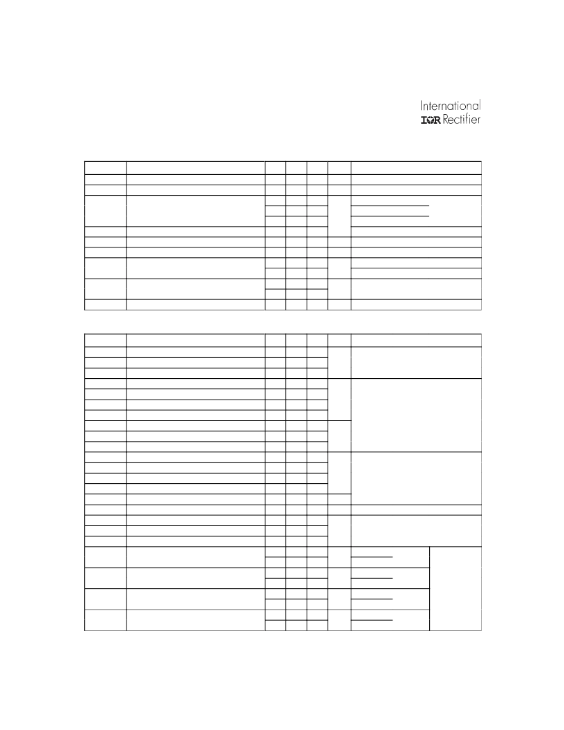
Parameter
Q
g
Total Gate Charge (turn-on)
Qge
Gate - Emitter Charge (turn-on)
Q
gc
Gate - Collector Charge (turn-on)
t
d(on)
Turn-On Delay Time
t
r
Rise Time
t
d(off)
Turn-Off Delay Time
t
f
Fall Time
E
on
Turn-On Switching Loss
E
off
Turn-Off Switching Loss
E
ts
Total Switching Loss
t
d(on)
Turn-On Delay Time
t
r
Rise Time
t
d(off)
Turn-Off Delay Time
t
f
Fall Time
E
ts
Total Switching Loss
L
E
Internal Emitter Inductance
C
ies
Input Capacitance
C
oes
Output Capacitance
C
res
Reverse Transfer Capacitance
t
rr
Diode Reverse Recovery Time
Min. Typ. Max. Units
–––
50
–––
8.1
–––
18
–––
40
–––
21
–––
91
–––
80
–––
0.38
–––
0.16
–––
0.54
–––
40
–––
22
–––
120
–––
180
–––
0.89
–––
7.5
–––
1100
–––
–––
73
–––
14
–––
42
–––
80
–––
3.5
–––
5.6
–––
80
–––
220
–––
180
–––
120
Conditions
I
C
= 12A
V
CC
= 400V
V
GE
= 15V
T
J
= 25
°
C
I
C
= 12A, V
CC
= 480V
V
GE
= 15V, R
G
= 23
Energy losses include "tail" and
diode reverse recovery.
See Fig. 9, 10, 11, 18
75
12
27
–––
–––
140
130
–––
–––
0.9
–––
–––
–––
–––
–––
–––
nC
See Fig. 8
ns
mJ
T
J
= 150
°
C, See Fig. 9, 10, 11, 18
I
C
= 12A, V
CC
= 480V
V
GE
= 15V, R
G
= 23
Energy losses include "tail" and
diode reverse recovery.
Measured 5mm from package
V
GE
= 0V
V
CC
= 30V
See Fig. 7
= 1.0MHz
T
J
= 25
°
C See Fig.
T
J
= 125
°
C 14 I
F
= 12A
T
J
= 25
°
C See Fig.
T
J
= 125
°
C 15 V
R
= 200V
T
J
= 25
°
C See Fig.
T
J
= 125
°
C 16 di/dt 200A/μs
T
J
= 25
°
C See Fig.
T
J
= 125
°
C 17
ns
mJ
nH
–––
–––
60
120
6.0
10
180
600
–––
–––
pF
ns
I
rr
Diode Peak Reverse Recovery Current
A
Q
rr
Diode Reverse Recovery Charge
nC
di
(rec)M
/dt
Diode Peak Rate of Fall of Recovery
During t
b
A/μs
Parameter
V
(BR)CES
Collector-to-Emitter Breakdown Voltage
600
V
(BR)CES
/
T
J
Temperature Coeff. of Breakdown Voltage
V
CE(on)
Collector-to-Emitter Saturation Voltage
Min. Typ. Max. Units
–––
–––
0.63
–––
1.95
–––
2.52
–––
2.09
3.0
–––
-11
3.1
8.6
–––
–––
–––
–––
2500
–––
1.4
–––
1.3
–––
–––
±100
Conditions
V
GE
= 0V, I
C
= 250μA
V
GE
= 0V, I
C
= 1.0mA
I
C
= 12A
I
C
= 23A
I
C
= 12A, T
J
= 150
°
C
V
CE
= V
GE
, I
C
= 250μA
–––
–––
2.1
–––
–––
6.0
–––
mV/
°
C V
CE
= V
GE
, I
C
= 250μA
–––
S
V
CE
= 100V, I
C
= 12A
250
μA
V
GE
= 0V, V
CE
= 600V
V
GE
= 0V, V
CE
= 600V, T
J
= 150
°
C
1.7
V
I
C
= 12A
1.6
I
C
= 12A, T
J
= 150
°
C
nA
V
GE
= ±20V
V
V/
°
C
V
GE
= 15V
See Fig. 2, 5
V
V
GE(th)
V
GE(th)
/
T
J
Temperature Coeff. of Threshold Voltage
–––
g
fe
Forward Transconductance
I
CES
Zero Gate Voltage Collector Current
Gate Threshold Voltage
V
FM
Diode Forward Voltage Drop
See Fig. 13
I
GES
Gate-to-Emitter Leakage Current
Switching Characteristics @ T
J
= 25°C (unless otherwise specified)
Electrical Characteristics @ T
J
= 25°C (unless otherwise specified)
Powered by ICminer.com Electronic-Library Service CopyRight 2003
相關PDF資料 |
PDF描述 |
|---|---|
| IRG4BAC50S | |
| IRG4BAC50U | |
| IRG4BAC50W | |
| IRG4BC10SD | TRANSISTOR | IGBT | N-CHAN | 600V V(BR)CES | 14A I(C) | TO-220AB |
| IRG4BC10SD-STRL | TRANSISTOR | IGBT | N-CHAN | 600V V(BR)CES | 14A I(C) | TO-263AB |
相關代理商/技術參數(shù) |
參數(shù)描述 |
|---|---|
| IRG4BAC50S | 制造商:未知廠家 制造商全稱:未知廠家 功能描述: |
| IRG4BAC50U | 制造商:未知廠家 制造商全稱:未知廠家 功能描述: |
| IRG4BAC50W | 制造商:未知廠家 制造商全稱:未知廠家 功能描述: |
| IRG4BAC50W-S | 功能描述:DIODE IGBT 600V SUPER 220 RoHS:否 類別:分離式半導體產(chǎn)品 >> IGBT - 單路 系列:- 標準包裝:30 系列:GenX3™ IGBT 類型:PT 電壓 - 集電極發(fā)射極擊穿(最大):1200V Vge, Ic時的最大Vce(開):3V @ 15V,100A 電流 - 集電極 (Ic)(最大):200A 功率 - 最大:830W 輸入類型:標準 安裝類型:通孔 封裝/外殼:TO-247-3 供應商設備封裝:PLUS247?-3 包裝:管件 |
| IRG4BAC50W-SPBF | 功能描述:IGBT N-CHAN 600V 55A SUPER220 RoHS:是 類別:分離式半導體產(chǎn)品 >> IGBT - 單路 系列:- 標準包裝:30 系列:GenX3™ IGBT 類型:PT 電壓 - 集電極發(fā)射極擊穿(最大):1200V Vge, Ic時的最大Vce(開):3V @ 15V,100A 電流 - 集電極 (Ic)(最大):200A 功率 - 最大:830W 輸入類型:標準 安裝類型:通孔 封裝/外殼:TO-247-3 供應商設備封裝:PLUS247?-3 包裝:管件 |
發(fā)布緊急采購,3分鐘左右您將得到回復。