- 您現在的位置:買賣IC網 > PDF目錄21974 > LFEC6E-3F256C (Lattice Semiconductor Corporation)IC FPGA 6.1KLUTS 195I/O 256-BGA PDF資料下載
參數資料
| 型號: | LFEC6E-3F256C |
| 廠商: | Lattice Semiconductor Corporation |
| 文件頁數: | 81/163頁 |
| 文件大小: | 0K |
| 描述: | IC FPGA 6.1KLUTS 195I/O 256-BGA |
| 標準包裝: | 90 |
| 系列: | EC |
| 邏輯元件/單元數: | 6100 |
| RAM 位總計: | 94208 |
| 輸入/輸出數: | 195 |
| 電源電壓: | 1.14 V ~ 1.26 V |
| 安裝類型: | 表面貼裝 |
| 工作溫度: | 0°C ~ 85°C |
| 封裝/外殼: | 256-BGA |
| 供應商設備封裝: | 256-FPBGA(17x17) |
| 其它名稱: | 220-1236 |
第1頁第2頁第3頁第4頁第5頁第6頁第7頁第8頁第9頁第10頁第11頁第12頁第13頁第14頁第15頁第16頁第17頁第18頁第19頁第20頁第21頁第22頁第23頁第24頁第25頁第26頁第27頁第28頁第29頁第30頁第31頁第32頁第33頁第34頁第35頁第36頁第37頁第38頁第39頁第40頁第41頁第42頁第43頁第44頁第45頁第46頁第47頁第48頁第49頁第50頁第51頁第52頁第53頁第54頁第55頁第56頁第57頁第58頁第59頁第60頁第61頁第62頁第63頁第64頁第65頁第66頁第67頁第68頁第69頁第70頁第71頁第72頁第73頁第74頁第75頁第76頁第77頁第78頁第79頁第80頁當前第81頁第82頁第83頁第84頁第85頁第86頁第87頁第88頁第89頁第90頁第91頁第92頁第93頁第94頁第95頁第96頁第97頁第98頁第99頁第100頁第101頁第102頁第103頁第104頁第105頁第106頁第107頁第108頁第109頁第110頁第111頁第112頁第113頁第114頁第115頁第116頁第117頁第118頁第119頁第120頁第121頁第122頁第123頁第124頁第125頁第126頁第127頁第128頁第129頁第130頁第131頁第132頁第133頁第134頁第135頁第136頁第137頁第138頁第139頁第140頁第141頁第142頁第143頁第144頁第145頁第146頁第147頁第148頁第149頁第150頁第151頁第152頁第153頁第154頁第155頁第156頁第157頁第158頁第159頁第160頁第161頁第162頁第163頁
2-21
Architecture
LatticeECP/EC Family Data Sheet
For further information about the sysDSP block, please see the list of technical information at the end of this data
sheet.
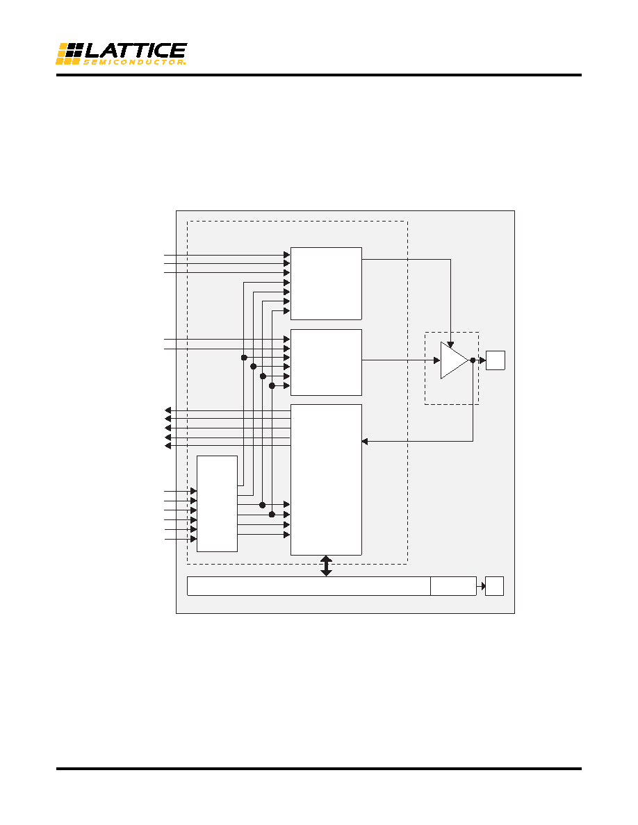
Programmable I/O Cells (PIC)
Each PIC contains two PIOs connected to their respective sysI/O Buffers which are then connected to the PADs as
shown in Figure 2-24. The PIO Block supplies the output data (DO) and the Tri-state control signal (TO) to sysI/O
buffer, and receives input from the buffer.
Figure 2-24. PIC Diagram
Two adjacent PIOs can be joined to provide a differential I/O pair (labeled as “T” and “C”) as shown in Figure 2-25.
The PAD Labels “T” and “C” distinguish the two PIOs. Only the PIO pairs on the left and right edges of the device
can be configured as LVDS transmit/receive pairs.
One of every 16 PIOs contains a delay element to facilitate the generation of DQS signals. The DQS signal feeds
the DQS bus which spans the set of 16 PIOs. Figure 2-25 shows the assignment of DQS pins in each set of 16
PIOs. The exact DQS pins are shown in a dual function in the Logic Signal Connections table at the end of this data
sheet. Additional detail is provided in the Signal Descriptions table at the end of this data sheet. The DQS signal
from the bus is used to strobe the DDR data from the memory into input register blocks. This interface is designed
for memories that support one DQS strobe per eight bits of data.
PIO B
PADA
"T"
PADB
"C"
OPOS0
ONEG0
OPOS1
ONEG1
TD
INCK
INDD
INFF
IPOS0
IPOS1
CLK
CE
LSR
GSRN
PIO A
sysIO
Buffer
DQS
DDRCLKPOL
IOLD0
IOLT0
D0
DDRCLK
DI
IPOS1
IPOS0
INCK
INDD
INFF
D0
D1
TD
D1
Output
Register Block
(2 Flip Flops)
Tristate
Register Block
(2 Flip Flops)
DDRCLK
Input
Register Block
(5 Flip Flops)
CLKO
CLKI
CEO
CEI
Control
Muxes
LSR
GSR
相關PDF資料 |
PDF描述 |
|---|---|
| VE-25R-CW-F3 | CONVERTER MOD DC/DC 7.5V 100W |
| REC3-1212DRW/H2/A | CONV DC/DC 3W 9-18VIN +/-12VOUT |
| LFXP10C-3FN388C | IC FPGA 9.7KLUTS 244I/O 388-BGA |
| FAN5345S20X | IC LED DVR ASYNC BOOST 20V 6SSOT |
| VI-B21-CY-S | CONVERTER MOD DC/DC 12V 50W |
相關代理商/技術參數 |
參數描述 |
|---|---|
| LFEC6E-3F256I | 功能描述:FPGA - 現場可編程門陣列 6.1 LUT 195 I/O RoHS:否 制造商:Altera Corporation 系列:Cyclone V E 柵極數量: 邏輯塊數量:943 內嵌式塊RAM - EBR:1956 kbit 輸入/輸出端數量:128 最大工作頻率:800 MHz 工作電源電壓:1.1 V 最大工作溫度:+ 70 C 安裝風格:SMD/SMT 封裝 / 箱體:FBGA-256 |
| LFEC6E-3F484C | 功能描述:FPGA - 現場可編程門陣列 6.1 LUT 224 I/O RoHS:否 制造商:Altera Corporation 系列:Cyclone V E 柵極數量: 邏輯塊數量:943 內嵌式塊RAM - EBR:1956 kbit 輸入/輸出端數量:128 最大工作頻率:800 MHz 工作電源電壓:1.1 V 最大工作溫度:+ 70 C 安裝風格:SMD/SMT 封裝 / 箱體:FBGA-256 |
| LFEC6E-3F484I | 功能描述:FPGA - 現場可編程門陣列 6.1 LUT 224 I/O RoHS:否 制造商:Altera Corporation 系列:Cyclone V E 柵極數量: 邏輯塊數量:943 內嵌式塊RAM - EBR:1956 kbit 輸入/輸出端數量:128 最大工作頻率:800 MHz 工作電源電壓:1.1 V 最大工作溫度:+ 70 C 安裝風格:SMD/SMT 封裝 / 箱體:FBGA-256 |
| LFEC6E-3F672C | 制造商:LATTICE 制造商全稱:Lattice Semiconductor 功能描述:LatticeECP/EC Family Data Sheet |
| LFEC6E-3F672I | 制造商:LATTICE 制造商全稱:Lattice Semiconductor 功能描述:LatticeECP/EC Family Data Sheet |
發布緊急采購,3分鐘左右您將得到回復。