- 您現在的位置:買賣IC網 > PDF目錄361030 > LM5642 (National Semiconductor Corporation) High Voltage, Dual Synchronous Buck Converter with Oscillator Synchronization PDF資料下載
參數資料
| 型號: | LM5642 |
| 廠商: | National Semiconductor Corporation |
| 英文描述: | High Voltage, Dual Synchronous Buck Converter with Oscillator Synchronization |
| 中文描述: | 高電壓,雙同步降壓轉換器振蕩器同步 |
| 文件頁數: | 15/24頁 |
| 文件大小: | 667K |
| 代理商: | LM5642 |
Operating Descriptions
(Continued)
capacitor through the inductor. To reset the OVP latch, either
the input voltage must be cycled, or both channels must be
switched off.
UNDER VOLTAGE PROTECTION (UVP) AND UV DELAY
If the output voltage on either channel falls below 80% of
nominal, under voltage protection activates. As shown in
Figure 5
, an under-voltage event will shut off the UV_DELAY
MOSFET, which will allow the UV_DELAY capacitor to
charge at 5μA (typical). At the UV_DELAY threshold (2.3V
typical) both channels will latch off. Also, UV_DELAY will be
disabled and the UV_DELAY pin will return to 0V. During
UVP, both the high side and low side FET drivers will be
turned off. If no capacitor is connected to the UV_DELAY pin,
the UVP latch will be activated immediately. To reset the
UVP latch, either the input voltage must be cycled, or both
ON/SS pins must be pulled low. The UVP function can be
disabled by connecting the UV_DELAY pin to ground.
THERMAL SHUTDOWN
The LM5642 IC will enter thermal shutdown if the die tem-
perature exceeds 160C. The top and bottom FETs of both
channels will be turned off immediately. In addition, both soft
capacitors will begin to discharge through separate 5.5μA
current sinks. The voltage on both capacitors will settle to
approximately 1.1V, where it will remain until the thermal
shutdown condition has cleared. The IC will return to normal
operating mode when the die temperature has fallen to
below 146C. At this point the two soft start capacitors will
begin to charge with their normal 2.4μAcurrent sources. This
allows a controlled return to normal operation, similar to the
soft start during turn-on. If the thermal shutdown condition
clears before the voltage on the soft start capacitors has
fallen to 1.1V, the capacitors will first be discharged to 1.1V,
and then immediately begin charging back up.
OUTPUT CAPACITOR DISCHARGE
Each channel has an embedded 480
MOSFET with the
drain connected to the SWx pin. This MOSFET will dis-
charge the output capacitor of its channel if its channel is off,
or the IC enters a fault state caused by one of the following
conditions:
1.
UVP
2.
UVLO
If an output over voltage event occurs, the HDRVx will be
turned off and LDRVx will be turned on immediately to
discharge the output capacitor of both channels through the
inductor.
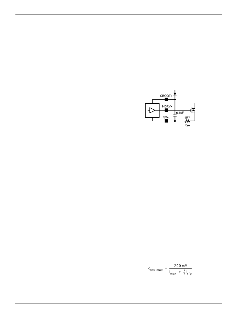
SWITCHING NOISE REDUCTION
Power MOSFETs are very fast switching devices. In syn-
chronous rectifier converters, the rapid increase of drain
current in the top FET coupled with parasitic inductance will
generate unwanted Ldi/dt noise spikes at the source node of
the FET (SWx node) and also at the VIN node. The magni-
tude of this noise will increase as the output current in-
creases. This parasitic spike noise may turn into electromag-
netic interference (EMI), and can also cause problems in
device performance. Therefore, it must be suppressed using
one of the following methods.
When using resistor sense, it is strongly recommended to
add R-C filters to the current sense amplifier inputs as shown
in
Figure 7
. This will reduce the susceptibility to switching
noise, especially during heavy load transients and short on
time conditions. The filter components should be connected
as close as possible to the IC.
As shown in
Figure 6
, adding a resistor in series with the
SWx pin will slow down the gate drive (HDRVx), thus slowing
the rise and fall time of the top FET, yielding a longer drain
current transition time.
Usually a 3.3
to 4.7
resistor is sufficient to suppress the
noise. Top FET switching losses will increase with higher
resistance values.
Small resistors (1-5 ohms) can also be placed in series with
the HDRVx pin or the CBOOTx pin to effectively reduce
switch node ringing. A CBOOT resistor will slow the rise time
of the FET, whereas a resistor at HDRV will reduce both rise
and fall times.
CURRENT SENSING AND LIMITING
As shown in
Figure 7
, the KSx and RSNSx pins are the
inputs of the current sense amplifier. Current sensing is
accomplished either by sensing the Vds of the top FET or by
sensing the voltage across a current sense resistor con-
nected from VIN to the drain of the top FET. The advantages
of sensing current across the top FET are reduced parts
count, cost and power loss.
The R
DS-ON
of the top FET is not as stable over temperature
and voltage as a sense resistor, hence great care must be
used in layout for V
DS
sensing circuits. At input voltages
above 30V, the maximum recommended output current is 5A
per channel.
Keeping the differential current-sense voltage below 200mV
ensures linear operation of the current sense amplifier.
Therefore, the R
of the top FET or the current sense
resistor must be small enough so that the current sense
voltage does not exceed 200mV when the top FET is on.
There is a leading edge blanking circuit that forces the top
FET on for at least 166ns. Beyond this minimum on time, the
output of the PWM comparator is used to turn off the top
FET. Additionally, a minimum voltage of at least 50mV
across Rsns is recommended to ensure a high SNR at the
current sense amplifier.
Assuming a maximum of 200mV across Rsns, the current
sense resistor can be calculated as follows:
(3)
where Imax is the maximum expected load current, including
overload multiplier (ie:120%), and Irip is the inductor ripple
current (See Equation 3). The above equation gives the
maximum allowable value for Rsns. Switching losses will
increase with Rsns, thus lowering efficiency.
20060109
FIGURE 6. SW Series Resistor
L
www.national.com
15
相關PDF資料 |
PDF描述 |
|---|---|
| LM5642MTC | High Voltage, Dual Synchronous Buck Converter with Oscillator Synchronization |
| LM565 | Phase Locked Loop |
| LM565C | |
| LM565CH | Analog Phase-Locked Loop |
| LM565CN | Phase Locked Loop |
相關代理商/技術參數 |
參數描述 |
|---|---|
| LM5642_07 | 制造商:NSC 制造商全稱:National Semiconductor 功能描述:High Voltage, Dual Synchronous Buck Converter with Oscillator Synchronization |
| LM5642EVAL-KIT | 功能描述:BOARD EVALUATION LM5642 RoHS:否 類別:編程器,開發系統 >> 評估板 - DC/DC 與 AC/DC(離線)SMPS 系列:PowerWise® 產品培訓模塊:Obsolescence Mitigation Program 標準包裝:1 系列:True Shutdown™ 主要目的:DC/DC,步升 輸出及類型:1,非隔離 功率 - 輸出:- 輸出電壓:- 電流 - 輸出:1A 輸入電壓:2.5 V ~ 5.5 V 穩壓器拓撲結構:升壓 頻率 - 開關:3MHz 板類型:完全填充 已供物品:板 已用 IC / 零件:MAX8969 |
| LM5642EVAL-KIT/NOPB | 功能描述:電源管理IC開發工具 LM5642 EVAL KIT RoHS:否 制造商:Maxim Integrated 產品:Evaluation Kits 類型:Battery Management 工具用于評估:MAX17710GB 輸入電壓: 輸出電壓:1.8 V |
| LM5642MH | 制造商:Texas Instruments 功能描述: |
| LM5642MH/NOPB | 功能描述:DC/DC 開關控制器 RoHS:否 制造商:Texas Instruments 輸入電壓:6 V to 100 V 開關頻率: 輸出電壓:1.215 V to 80 V 輸出電流:3.5 A 輸出端數量:1 最大工作溫度:+ 125 C 安裝風格: 封裝 / 箱體:CPAK |
發布緊急采購,3分鐘左右您將得到回復。