- 您現(xiàn)在的位置:買(mǎi)賣(mài)IC網(wǎng) > PDF目錄361030 > LM5642 (National Semiconductor Corporation) High Voltage, Dual Synchronous Buck Converter with Oscillator Synchronization PDF資料下載
參數(shù)資料
| 型號(hào): | LM5642 |
| 廠商: | National Semiconductor Corporation |
| 英文描述: | High Voltage, Dual Synchronous Buck Converter with Oscillator Synchronization |
| 中文描述: | 高電壓,雙同步降壓轉(zhuǎn)換器振蕩器同步 |
| 文件頁(yè)數(shù): | 19/24頁(yè) |
| 文件大小: | 667K |
| 代理商: | LM5642 |
第1頁(yè)第2頁(yè)第3頁(yè)第4頁(yè)第5頁(yè)第6頁(yè)第7頁(yè)第8頁(yè)第9頁(yè)第10頁(yè)第11頁(yè)第12頁(yè)第13頁(yè)第14頁(yè)第15頁(yè)第16頁(yè)第17頁(yè)第18頁(yè)當(dāng)前第19頁(yè)第20頁(yè)第21頁(yè)第22頁(yè)第23頁(yè)第24頁(yè)
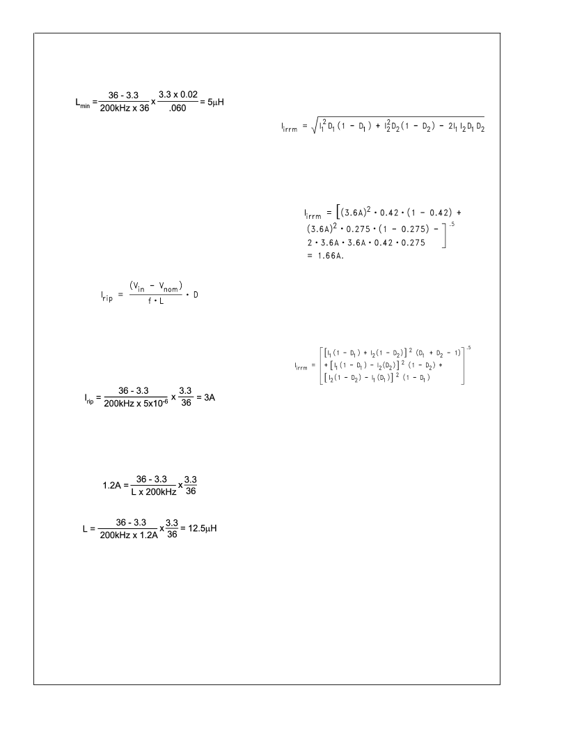
Inductor Selection
(Continued)
Example:
Vin = 36V, Vo = 3.3V, V
RIP
= 60mV, Re = 20m
,
F = 200kHz.
(16)
The actual selection process usually involves several itera-
tions of all of the above steps, from ripple voltage selection,
to capacitor selection, to inductance calculations. Both the
highest and the lowest input and output voltages and load
transient requirements should be considered. If an induc-
tance value larger than Lmin is selected, make sure that the
Cmin requirement is not violated.
Priority should be given to parameters that are not flexible or
more costly. For example, if there are very few types of
capacitors to choose from, it may be a good idea to adjust
the inductance value so that a requirement of 3.2 capacitors
can be reduced to 3 capacitors.
Since inductor ripple current is often the criterion for select-
ing an output inductor, it is a good idea to double-check this
value. The equation is:
(17)
Also important is the ripple content, which is defined by Irip
/Inom. Generally speaking, a ripple content of less than 50%
is ok. Larger ripple content will cause too much loss in the
inductor.
Example:
Vin = 36V, Vo = 3.3V, F = 200kHz, L = 5μH, 3A
max I
OUT
(18)
3A is 100% ripple which is too high.
In this case, the inductor should be reselected on the basis
of ripple current.
Example:
40% ripple, 40%
3A = 1.2A
(19)
(20)
When choosing the inductor, the saturation current should
be higher than the maximum peak inductor current and the
RMS current rating should be higher than the maximum load
current.
Input Capacitor Selection
The fact that the two switching channels of the LM5642 are
180 out of phase will reduce the RMS value of the ripple
current seen by the input capacitors. This will help extend
input capacitor life span and result in a more efficient sys-
tem. Input capacitors must be selected that can handle both
the maximum ripple RMS current at highest ambient tem-
perature as well as the maximum input voltage. In applica-
tions in which output voltages are less than half of the input
voltage, the corresponding duty cycles will be less than 50%.
This means there will be no overlap between the two chan-
nels’ input current pulses. The equation for calculating the
maximum total input ripple RMS current for duty cycles
under 50% is:
(21)
where I1 is maximum load current of Channel 1, I2 is the
maximum load current of Channel 2, D1 is the duty cycle of
Channel 1, and D2 is the duty cycle of Channel 2.
Example: Imax_1 = 3.6A, Imax_2 = 3.6A, D1 = 0.42, and D2
= 0.275
(22)
Choose input capacitors that can handle 1.66A ripple RMS
current at highest ambient temperature. In applications
where output voltages are greater than half the input voltage,
the corresponding duty cycles will be greater than 50%, and
there will be overlapping input current pulses. Input ripple
current will be highest under these circumstances. The input
RMS current in this case is given by:
(23)
Where, again, I1 and I2 are the maximum load currents of
channel 1 and 2, and D1 and D2 are the duty cycles. This
equation should be used when both duty cycles are ex-
pected to be higher than 50%.
If the LM5642 is being used with an external clock frequency
other than 200kHz, the preceding equations for input rms
current can still be used. The selection of the first equation or
the second changes because overlap can now occur at duty
cycles that are less than 50%. From the External Frequency
Sync section, the maximum duty cycle that ensures no over-
lap between duty cycles (and hence input current pulses) is:
D
MAX
= F
SYNC*
2.5 x 10
-6
There are now three distinct possibilities which must be
considered when selecting the equation for input rms cur-
rent:
1.
Both duty cycles D
and D
are less than D
. In this
case, the first, simple equation can always be used.
2.
One duty cycle is greater than D
and the other duty
cycle is less than D
. In this case, the system de-
signer can take advantage of the fact that the sync
feature reduces D
for one channel, but lengthens it
for the other channel. For F
<
200kHz, D
is re-
duced to D
MAX
while D
2
actually increases to (1-D
).
For F
200kHz, D
is reduced to D
while D
1
increases to (1-D
). By using the channel reduced to
D
for the lower duty cycle, and the channel that has
been increased for the higher duty cycle, the first, simple
rms input current equation can be used.
(24)
L
www.national.com
19
相關(guān)PDF資料 |
PDF描述 |
|---|---|
| LM5642MTC | High Voltage, Dual Synchronous Buck Converter with Oscillator Synchronization |
| LM565 | Phase Locked Loop |
| LM565C | |
| LM565CH | Analog Phase-Locked Loop |
| LM565CN | Phase Locked Loop |
相關(guān)代理商/技術(shù)參數(shù) |
參數(shù)描述 |
|---|---|
| LM5642_07 | 制造商:NSC 制造商全稱(chēng):National Semiconductor 功能描述:High Voltage, Dual Synchronous Buck Converter with Oscillator Synchronization |
| LM5642EVAL-KIT | 功能描述:BOARD EVALUATION LM5642 RoHS:否 類(lèi)別:編程器,開(kāi)發(fā)系統(tǒng) >> 評(píng)估板 - DC/DC 與 AC/DC(離線(xiàn))SMPS 系列:PowerWise® 產(chǎn)品培訓(xùn)模塊:Obsolescence Mitigation Program 標(biāo)準(zhǔn)包裝:1 系列:True Shutdown™ 主要目的:DC/DC,步升 輸出及類(lèi)型:1,非隔離 功率 - 輸出:- 輸出電壓:- 電流 - 輸出:1A 輸入電壓:2.5 V ~ 5.5 V 穩(wěn)壓器拓?fù)浣Y(jié)構(gòu):升壓 頻率 - 開(kāi)關(guān):3MHz 板類(lèi)型:完全填充 已供物品:板 已用 IC / 零件:MAX8969 |
| LM5642EVAL-KIT/NOPB | 功能描述:電源管理IC開(kāi)發(fā)工具 LM5642 EVAL KIT RoHS:否 制造商:Maxim Integrated 產(chǎn)品:Evaluation Kits 類(lèi)型:Battery Management 工具用于評(píng)估:MAX17710GB 輸入電壓: 輸出電壓:1.8 V |
| LM5642MH | 制造商:Texas Instruments 功能描述: |
| LM5642MH/NOPB | 功能描述:DC/DC 開(kāi)關(guān)控制器 RoHS:否 制造商:Texas Instruments 輸入電壓:6 V to 100 V 開(kāi)關(guān)頻率: 輸出電壓:1.215 V to 80 V 輸出電流:3.5 A 輸出端數(shù)量:1 最大工作溫度:+ 125 C 安裝風(fēng)格: 封裝 / 箱體:CPAK |
發(fā)布緊急采購(gòu),3分鐘左右您將得到回復(fù)。