- 您現在的位置:買賣IC網 > PDF目錄382290 > MBT35200 (ON SEMICONDUCTOR) 30 AMP MINIATURE POWER RELAY PDF資料下載
參數資料
| 型號: | MBT35200 |
| 廠商: | ON SEMICONDUCTOR |
| 元件分類: | 繼電器,輸入/輸出模塊 |
| 英文描述: | 30 AMP MINIATURE POWER RELAY |
| 中文描述: | 高電流表面貼裝進步黨硅晶體管的負荷開關在便攜式應用管理 |
| 文件頁數: | 5/8頁 |
| 文件大小: | 81K |
| 代理商: | MBT35200 |
MBT35200MT1
http://onsemi.com
5
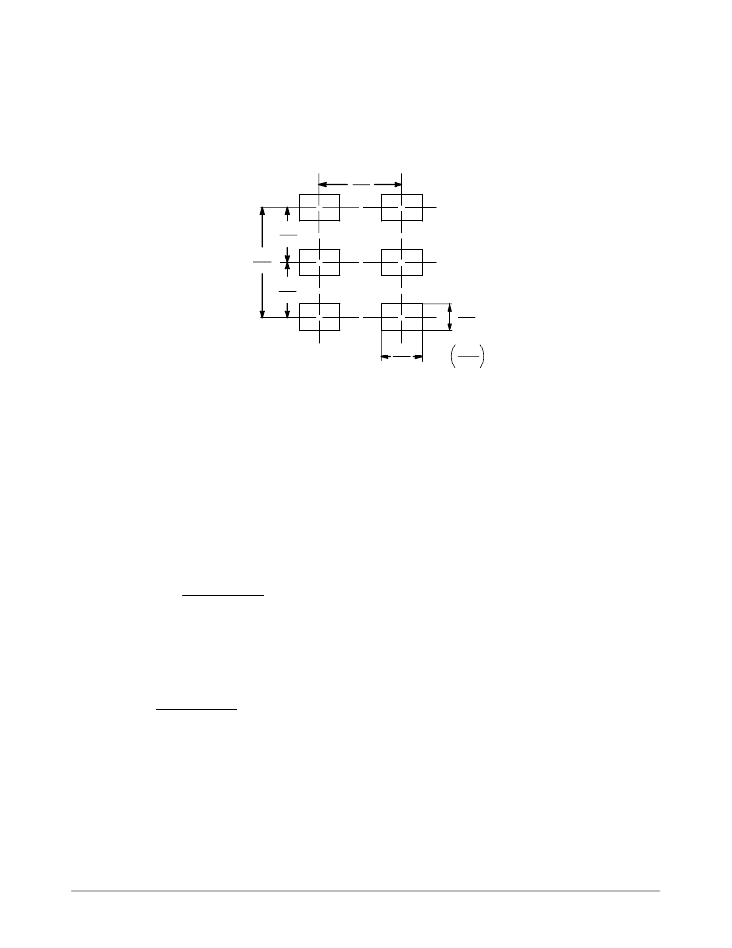
INFORMATION FOR USING THE TSOP–6 SURFACE MOUNT PACKAGE
MINIMUM RECOMMENDED FOOTPRINT FOR SURFACE MOUNTED APPLICATIONS
Surface mount board layout is a critical portion of the
total design. The footprint for the semiconductor packages
must be the correct size to insure proper solder connection
interface between the board and the package. With the
correct pad geometry, the packages will self align when
subjected to a solder reflow process.
mm
inches
1.9
0.039
1.0
0.094
2.4
0.7
0.074
0.028
0.95
0.037
0.95
0.037
TSOP–6
TSOP–6 POWER DISSIPATION
The power dissipation of the TSOP–6 is a function of the
drain pad size. This can vary from the minimum pad size
for soldering to a pad size given for maximum power
dissipation. Power dissipation for a surface mount device is
determined by T
J(max)
, the maximum rated junction
temperature of the die, R
θ
JA
, the thermal resistance from
the device junction to ambient, and the operating
temperature, T
A
. Using the values provided on the data
sheet for the TSOP–6 package, P
D
can be calculated as
follows:
P
D
=
T
J(max)
– T
A
R
θ
JA
The values for the equation are found in the maximum
ratings table on the data sheet. Substituting these values
into the equation for an ambient temperature T
A
of 25
°
C,
one can calculate the power dissipation of the device which
in this case is 625 milliwatts.
P
D
=
150
°
C – 25
°
C
200
°
C/W
= 625 milliwatts
The 200
°
C/W for the TSOP–6 package assumes the use
of the recommended footprint on a glass epoxy printed
circuit board to achieve a power dissipation of
625 milliwatts. There are other alternatives to achieving
higher power dissipation from the TSOP–6 package.
Another alternative would be to use a ceramic substrate or
an aluminum core board such as Thermal Clad
. Using a
board material such as Thermal Clad, an aluminum core
board, the power dissipation can be doubled using the same
footprint.
SOLDERING PRECAUTIONS
The melting temperature of solder is higher than the rated
temperature of the device. When the entire device is heated
to a high temperature, failure to complete soldering within
a short time could result in device failure. Therefore, the
following items should always be observed in order to
minimize the thermal stress to which the devices are
subjected.
Always preheat the device.
The delta temperature between the preheat and
soldering should be 100
°
C or less.*
When preheating and soldering, the temperature of the
leads and the case must not exceed the maximum
temperature ratings as shown on the data sheet. When
using infrared heating with the reflow soldering
method, the difference shall be a maximum of 10
°
C.
The soldering temperature and time shall not exceed
260
°
C for more than 10 seconds.
When shifting from preheating to soldering, the
maximum temperature gradient shall be 5
°
C or less.
After soldering has been completed, the device should
be allowed to cool naturally for at least three minutes.
Gradual cooling should be used as the use of forced
cooling will increase the temperature gradient and
result in latent failure due to mechanical stress.
Mechanical stress or shock should not be applied
during cooling.
* Soldering a device without preheating can cause
excessive thermal shock and stress which can result in
damage to the device.
相關PDF資料 |
PDF描述 |
|---|---|
| MBT3906DW1T1 | Dual General Purpose Transistor |
| MBT3906DW1T1G | Dual General Purpose Transistor |
| MBT3906DW1T1 | Dual General Purpose Transistors |
| MC100EP16TDT | 3.3V / 5V ECL Differential Receiver/Driver with Internal Termination |
| MC100EP16VC | 3.3V / 5V ECL Differential Receiver/Driver with High Gain and Enable Output |
相關代理商/技術參數 |
參數描述 |
|---|---|
| MBT35200MT1 | 功能描述:兩極晶體管 - BJT Low Saturation RoHS:否 制造商:STMicroelectronics 配置: 晶體管極性:PNP 集電極—基極電壓 VCBO: 集電極—發射極最大電壓 VCEO:- 40 V 發射極 - 基極電壓 VEBO:- 6 V 集電極—射極飽和電壓: 最大直流電集電極電流: 增益帶寬產品fT: 直流集電極/Base Gain hfe Min:100 A 最大工作溫度: 安裝風格:SMD/SMT 封裝 / 箱體:PowerFLAT 2 x 2 |
| MBT35200MT1_05 | 制造商:ONSEMI 制造商全稱:ON Semiconductor 功能描述:High Current Surface Mount PNP Silicon Switching Transistor for Load Management in Portable Applications |
| MBT35200MT1G | 功能描述:兩極晶體管 - BJT Low Saturation RoHS:否 制造商:STMicroelectronics 配置: 晶體管極性:PNP 集電極—基極電壓 VCBO: 集電極—發射極最大電壓 VCEO:- 40 V 發射極 - 基極電壓 VEBO:- 6 V 集電極—射極飽和電壓: 最大直流電集電極電流: 增益帶寬產品fT: 直流集電極/Base Gain hfe Min:100 A 最大工作溫度: 安裝風格:SMD/SMT 封裝 / 箱體:PowerFLAT 2 x 2 |
| MBT35200MT1G | 制造商:ON Semiconductor 功能描述:Bipolar Transistor |
| MBT35200MT2G | 功能描述:兩極晶體管 - BJT TSOP6 PNP XSTR SPCL RoHS:否 制造商:STMicroelectronics 配置: 晶體管極性:PNP 集電極—基極電壓 VCBO: 集電極—發射極最大電壓 VCEO:- 40 V 發射極 - 基極電壓 VEBO:- 6 V 集電極—射極飽和電壓: 最大直流電集電極電流: 增益帶寬產品fT: 直流集電極/Base Gain hfe Min:100 A 最大工作溫度: 安裝風格:SMD/SMT 封裝 / 箱體:PowerFLAT 2 x 2 |
發布緊急采購,3分鐘左右您將得到回復。