- 您現在的位置:買賣IC網 > PDF目錄371048 > MC68HC11A1CFN2 (MOTOROLA INC) HCMOS Single-Chip Microcontroller PDF資料下載
參數資料
| 型號: | MC68HC11A1CFN2 |
| 廠商: | MOTOROLA INC |
| 元件分類: | 微控制器/微處理器 |
| 英文描述: | HCMOS Single-Chip Microcontroller |
| 中文描述: | 8-BIT, 2 MHz, MICROCONTROLLER, PQCC52 |
| 封裝: | PLASTIC, LCC-52 |
| 文件頁數: | 60/158頁 |
| 文件大小: | 776K |
| 代理商: | MC68HC11A1CFN2 |
第1頁第2頁第3頁第4頁第5頁第6頁第7頁第8頁第9頁第10頁第11頁第12頁第13頁第14頁第15頁第16頁第17頁第18頁第19頁第20頁第21頁第22頁第23頁第24頁第25頁第26頁第27頁第28頁第29頁第30頁第31頁第32頁第33頁第34頁第35頁第36頁第37頁第38頁第39頁第40頁第41頁第42頁第43頁第44頁第45頁第46頁第47頁第48頁第49頁第50頁第51頁第52頁第53頁第54頁第55頁第56頁第57頁第58頁第59頁當前第60頁第61頁第62頁第63頁第64頁第65頁第66頁第67頁第68頁第69頁第70頁第71頁第72頁第73頁第74頁第75頁第76頁第77頁第78頁第79頁第80頁第81頁第82頁第83頁第84頁第85頁第86頁第87頁第88頁第89頁第90頁第91頁第92頁第93頁第94頁第95頁第96頁第97頁第98頁第99頁第100頁第101頁第102頁第103頁第104頁第105頁第106頁第107頁第108頁第109頁第110頁第111頁第112頁第113頁第114頁第115頁第116頁第117頁第118頁第119頁第120頁第121頁第122頁第123頁第124頁第125頁第126頁第127頁第128頁第129頁第130頁第131頁第132頁第133頁第134頁第135頁第136頁第137頁第138頁第139頁第140頁第141頁第142頁第143頁第144頁第145頁第146頁第147頁第148頁第149頁第150頁第151頁第152頁第153頁第154頁第155頁第156頁第157頁第158頁
MOTOROLA
6-2
SERIAL PERIPHERAL INTERFACE
MC68HC11A8
TECHNICAL DATA
6
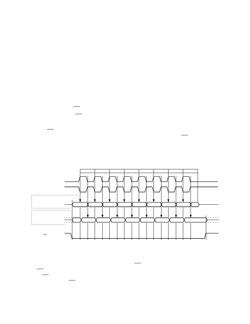
6.2.3 Serial Clock (SCK)
The serial clock is used to synchronize data movement both in and out of the device
through its MOSI and MISO lines. The master and slave devices are capable of ex-
changing a byte of information during a sequence of eight clock cycles. Since SCK is
generated by the master device, this line becomes an input on a slave device.
As shown in
Figure 6-1
, four possible timing relationships may be chosen by using
control bits CPOL and CPHA in the serial peripheral control register (SPCR). Both
master and slave devices must operate with the same timing. The master device al-
ways places data on the MOSI line a half-cycle before the clock edge (SCK), in order
for the slave device to latch the data.
Two bits (SPR0 and SPR1) in the SPCR of the master device select the clock rate. In
a slave device, SPR0 and SPR1 have no effect on the operation of the SPI.
6.2.4 Slave Select (SS)
The slave select (SS) input line is used to select a slave device. It has to be low prior
to data transactions and must stay low for the duration of the transaction.
The SS line on the master must be tied high. If it goes low, a mode fault error flag
(MODF) is set in the serial peripheral status register (SPSR). The SS pin can be se-
lected to be a general-purpose output by writing a one in bit 5 of the port D data direc-
tion register, thus disabling the mode fault circuit. The other three SPI lines are
dedicated to the SPI whenever the SPI is on.
Figure 6-1 Data Clock Timing Diagram
When CPHA = 0, the shift clock is the OR of SS with SCK. In this clock phase mode,
SS must go high between successive characters in an SPI message. When CPHA =
1, SS may be left low for several SPI characters. In cases where there is only one SPI
slave MCU, its SS line could be tied to V
SS
as long as CPHA = 1 clock modes are used.
SCK CYCLE #
(FOR REFERENCE)
1
2
3
4
5
6
7
8
SCK (CPOL = 0)
SCK (CPOL = 1)
(CPHA = 0) DATA OUT
(CPHA = 1) DATA OUT
SS (TO SLAVE)
SAMPLE INPUT
SAMPLE INPUT
MSB
6
5
4
3
2
1
LSB
MSB
6
5
4
3
2
1
LSB
SPI TRANSFER FORMAT
相關PDF資料 |
PDF描述 |
|---|---|
| MC68HCP11A1CFN2 | HCMOS Single-Chip Microcontroller |
| MC68HCP11A1CFN3 | HCMOS Single-Chip Microcontroller |
| MC68HCP11A1CP2 | HCMOS Single-Chip Microcontroller |
| MC68HCP11A1CP3 | HCMOS Single-Chip Microcontroller |
| MC68HCP11A1MFN2 | HCMOS Single-Chip Microcontroller |
相關代理商/技術參數 |
參數描述 |
|---|---|
| MC68HC11A1CFN3 | 制造商:Rochester Electronics LLC 功能描述: |
| MC68HC11A1CFNE3 | 功能描述:8位微控制器 -MCU 8B MCU 256RAM A/D EE RoHS:否 制造商:Silicon Labs 核心:8051 處理器系列:C8051F39x 數據總線寬度:8 bit 最大時鐘頻率:50 MHz 程序存儲器大小:16 KB 數據 RAM 大小:1 KB 片上 ADC:Yes 工作電源電壓:1.8 V to 3.6 V 工作溫度范圍:- 40 C to + 105 C 封裝 / 箱體:QFN-20 安裝風格:SMD/SMT |
| MC68HC11A1CFNE3 | 制造商:Freescale Semiconductor 功能描述:8-BIT MICROCONTROLLER IC |
| MC68HC11A1CFNE3R | 功能描述:8位微控制器 -MCU 8B MCU 256RAM A/D EE RoHS:否 制造商:Silicon Labs 核心:8051 處理器系列:C8051F39x 數據總線寬度:8 bit 最大時鐘頻率:50 MHz 程序存儲器大小:16 KB 數據 RAM 大小:1 KB 片上 ADC:Yes 工作電源電壓:1.8 V to 3.6 V 工作溫度范圍:- 40 C to + 105 C 封裝 / 箱體:QFN-20 安裝風格:SMD/SMT |
| MC68HC11A1CFU2 | 制造商:MOTOROLA 制造商全稱:Motorola, Inc 功能描述:HCMOS Single-Chip Microcontroller |
發布緊急采購,3分鐘左右您將得到回復。