- 您現在的位置:買賣IC網 > PDF目錄382345 > MPC9229 (Motorola, Inc.) 400 MHz Low Voltage PECL Clock Synthesizer PDF資料下載
參數資料
| 型號: | MPC9229 |
| 廠商: | Motorola, Inc. |
| 英文描述: | 400 MHz Low Voltage PECL Clock Synthesizer |
| 中文描述: | 400 MHz低電壓PECL時鐘合成器 |
| 文件頁數: | 8/12頁 |
| 文件大小: | 366K |
| 代理商: | MPC9229 |
MPC9229
MOTOROLA
TIMING SOLUTIONS
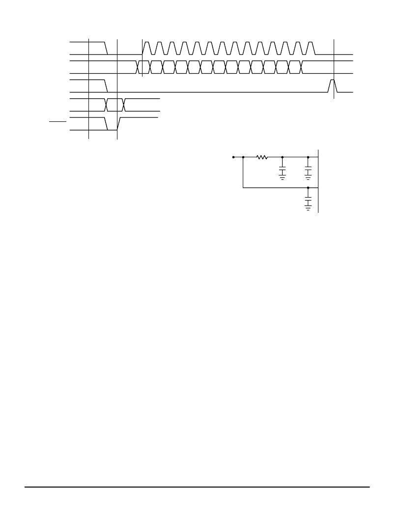
Figure 4. Serial Interface Timing Diagram
S_CLOCK
S_DATA
S_LOAD
M[8:0]
N[1:0]
P_LOAD
T2
T1
T0
N1
N0
M8
M7
M6
M5
M4
M3
M2
M1
M0
M, N
First
Bit
Last
Bit
Power Supply Filtering
The MPC9229 is a mixed analog/digital product. Its analog
circuitry is naturally susceptible to random noise, especially if
this noise is seen on the powersupply pins.Random noise on
the VCC_PLL pin impacts the device characteristics. The
MPC9229 provides separate power supplies for the digital
circuitry (VCC) and the internalPLL (VCC_PLL)of the device.
The purpose of this design technique is to try and isolate the
high switching noise digital outputs from the relatively
sensitive internal analog phase–locked loop. In a controlled
environment such as an evaluation board, this level of
isolationissufficient.However,inadigitalsystemenvironment
where it is more difficult to minimize noise on the power
supplies a second level of isolation may be required. The
simplest form of isolation is a power supply filter on the
VCC_PLL pin for the MPC9229. Figure 5 illustrates a typical
powersupplyfilterscheme.TheMPC9229ismostsusceptible
to noise with spectral content in the 1 kHz to 1 MHz range.
Therefore, the filter should be designed to target this range.
Thekeyparameterthatneedstobemetinthefinalfilterdesign
is the DC voltage drop that will be seen between the VCC
supply and the MPC9229 pin of the MPC9229. From the data
sheet, the VCC_PLL current (the current sourced through the
VCC_PLL pin) is maximum 20 mA, assuming that a minimum
of 2.835 V must be maintained on the VCC_PLL pin. The
resistor shown in Figure 5 must have a resistance of 10-15
to meet the voltage drop criteria. The RC filter pictured will
provide
a
broadband
filter
attenuation fornoise whose spectral contentis above 20 kHz.
Asthenoisefrequencycrosses theseries resonantpointofan
individual capacitor its overall impedance begins to look
inductive and thus increases with increasing frequency. The
parallel capacitor combination shown ensures that a low
impedance path to ground exists for frequencies well above
the bandwidth of the PLL. Generally, the resistor/capacitor
filter will be cheaper, easier to implement and provide an
adequate level of supply filtering. A higher level ofattenuation
can be achieved by replacing the resistor with an appropriate
valued inductor. A 1000
μ
H choke will show a significant
impedance at 10 kHz frequencies and above. Because of the
current draw and the voltage that must be maintained on the
VCC_PLL pin, a low DC resistance inductor is required (less
than 15
).
with
approximately
100:1
Figure 5. V
CC PLL
Power Supply Filter
VCC_PLL
V
CC
MPC9229
C
1
, C
2
= 0.01...0.1
μ
F
V
CC
C
F
= 22
μ
F
R
F
= 10--15
C
2
C
1
Layout Recommendations
The MPC9229 provides sub–nanosecond output edge
rates and thus a good power supply bypassing scheme is a
must. Figure 6 shows a representative board layout for the
MPC9229.Thereexistsmany differentpotentialboardlayouts
and the one pictured is but one. The important aspect of the
layout in Figure 6 is the low impedance connections between
VCC and GND for the bypass capacitors. Combining good
quality generalpurpose chip capacitors with good PCBlayout
techniques will produce effective capacitor resonances at
frequencies adequate to supply the instantaneous switching
current for the MPC9229 outputs. It is imperative that low
inductance chip capacitors are used; it is equally important
that the board layout does not introduce back all of the
inductance saved by using the leadless capacitors. Thin
interconnect traces between the capacitor and the power
plane should be avoided and multiple large vias should be
used to tie the capacitors to the buried power planes. Fat
interconnect and large vias will help to minimize layout
induced inductance and thus maximize the series resonant
point of the bypass capacitors. Note the dotted lines circling
the crystaloscillatorconnection to the device.The oscillatoris
a series resonant circuit and the voltage amplitude across the
crystal is relatively small. It is imperative that no actively
switching signals cross under the crystal as crosstalk energy
coupled to these lines could significantlyimpactthejitterofthe
device. Special attention should be paid to the layout of the
crystal to ensure a stable, jitter free interface between the
crystal and the on–board oscillator. Although the MPC9229
has several design features to minimize the susceptibility to
F
Freescale Semiconductor, Inc.
For More Information On This Product,
Go to: www.freescale.com
n
.
相關PDF資料 |
PDF描述 |
|---|---|
| MPC9230 | 800 MHz Low Voltage PECL Clock Synthesizer |
| MPC9350 | LOW VOLTAGE PLL CLOCK DRIVER |
| MPC9350D | LOW VOLTAGE PLL CLOCK DRIVER |
| MPC9446 | 2.5V and 3.3V LVCMOS Clock Fanout Buffer |
| MPC9448 | 3.3V/2.5V LVCMOS 1:12 Clock Fanout Buffer |
相關代理商/技術參數 |
參數描述 |
|---|---|
| MPC9229AC | 功能描述:時鐘合成器/抖動清除器 FSL 400MHz LVPECL Freq. Synthesizer RoHS:否 制造商:Skyworks Solutions, Inc. 輸出端數量: 輸出電平: 最大輸出頻率: 輸入電平: 最大輸入頻率:6.1 GHz 電源電壓-最大:3.3 V 電源電壓-最小:2.7 V 封裝 / 箱體:TSSOP-28 封裝:Reel |
| MPC9229ACR2 | 功能描述:時鐘合成器/抖動清除器 FSL 400MHz LVPECL Freq. Synthesizer RoHS:否 制造商:Skyworks Solutions, Inc. 輸出端數量: 輸出電平: 最大輸出頻率: 輸入電平: 最大輸入頻率:6.1 GHz 電源電壓-最大:3.3 V 電源電壓-最小:2.7 V 封裝 / 箱體:TSSOP-28 封裝:Reel |
| MPC9229EI | 功能描述:時鐘合成器/抖動清除器 FSL 400MHz LVPECL Freq. Synthesizer RoHS:否 制造商:Skyworks Solutions, Inc. 輸出端數量: 輸出電平: 最大輸出頻率: 輸入電平: 最大輸入頻率:6.1 GHz 電源電壓-最大:3.3 V 電源電壓-最小:2.7 V 封裝 / 箱體:TSSOP-28 封裝:Reel |
| MPC9229EIR2 | 功能描述:時鐘合成器/抖動清除器 FSL 400MHz LVPECL Freq. Synthesizer RoHS:否 制造商:Skyworks Solutions, Inc. 輸出端數量: 輸出電平: 最大輸出頻率: 輸入電平: 最大輸入頻率:6.1 GHz 電源電壓-最大:3.3 V 電源電壓-最小:2.7 V 封裝 / 箱體:TSSOP-28 封裝:Reel |
| MPC9229FA | 功能描述:IC PECL CLOCK LV 400MHZ 32-LQFP RoHS:否 類別:集成電路 (IC) >> 時鐘/計時 - 時鐘發生器,PLL,頻率合成器 系列:- 標準包裝:39 系列:- 類型:* PLL:帶旁路 輸入:時鐘 輸出:時鐘 電路數:1 比率 - 輸入:輸出:1:10 差分 - 輸入:輸出:是/是 頻率 - 最大:170MHz 除法器/乘法器:無/無 電源電壓:2.375 V ~ 3.465 V 工作溫度:0°C ~ 70°C 安裝類型:* 封裝/外殼:* 供應商設備封裝:* 包裝:* |
發布緊急采購,3分鐘左右您將得到回復。