- 您現在的位置:買賣IC網 > PDF目錄382345 > MPC9448D (Motorola, Inc.) 3.3V/2.5V LVCMOS 1:12 Clock Fanout Buffer PDF資料下載
參數資料
| 型號: | MPC9448D |
| 廠商: | Motorola, Inc. |
| 英文描述: | 3.3V/2.5V LVCMOS 1:12 Clock Fanout Buffer |
| 中文描述: | 3.3V/2.5V的LVCMOS 1:12時鐘扇出緩沖器 |
| 文件頁數: | 7/12頁 |
| 文件大小: | 263K |
| 代理商: | MPC9448D |
MPC9448
TIMING SOLUTIONS
7
MOTOROLA
Since this step is well above the threshold region it will not
cause any false clock triggering; however, designers may be
uncomfortable with unwanted reflections on the line.
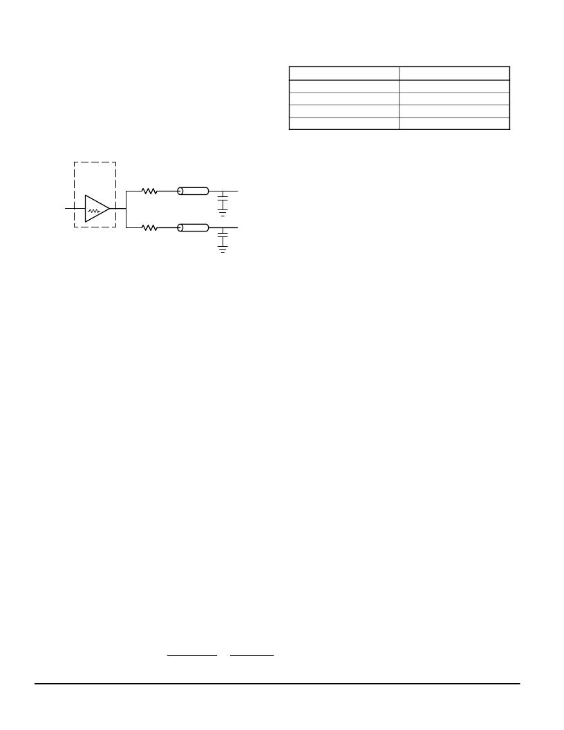
better match the impedances when driving multiple lines, the
situation in Figure 6 “Optimized Dual Line Termination”
should be used. In this case, the series terminating resistors
are reduced such that when the parallel combination is added
to the output buffer impedance the line impedance is
perfectly matched.
To
Figure 6. Optimized Dual Line Termination
17
MPC9448
OUTPUT
BUFFER
R
S
= 16
Z
O
= 50
R
S
= 16
Z
O
= 50
17
+ 16
k
16
= 50
k
50
25
= 25
Power Consumption of the MPC9448 and Thermal
Management
The MPC9448 AC specification is guaranteed for the
entire operating frequency range up to 350 MHz. The
MPC9448 power consumption and the associated long-term
reliability may decrease the maximum frequency limit,
depending on operating conditions such as clock frequency,
supply voltage, output loading, ambient temperture, vertical
convection and thermal conductivity of package and board.
This section describes the impact of these parameters on the
junction temperature and gives a guideline to estimate the
MPC9448 die junction temperature and the associated
device reliability. For a complete analysis of power
consumption as a function of operating conditions and
associated long term device reliability please refer to the
application note AN1545. According the AN1545, the
long-term device reliability is a function of the die junction
temperature:
Table 9. Die junction temperature and MTBF
Junction temperature (
°
C)
MTBF (Years)
100
110
120
130
20.4
9.1
4.2
2.0
Increased power consumption will increase the die
junction temperature and impact the device reliability
(MTBF). According to the system-defined tolerable MTBF,
the die junction temperature of the MPC9448 needs to be
controlled and the thermal impedance of the board/package
should be optimized. The power dissipated in the MPC9448
is represented in equation 1.
Where I
CCQ
is the static current consumption of the
MPC9448, C
PD
is the power dissipation capacitance per
output,
(Μ)Σ
C
L
represents the external capacitive output
load, N is the number of active outputs (N is always 12 in
case of the MPC9448). The MPC9448 supports driving
transmission lines to maintain high signal integrity and tight
timing parameters. Any transmission line will hide the lumped
capacitive load at the end of the board trace, therefore,
Σ
C
L
is
zero for controlled transmission line systems and can be
eliminated from equation 1. Using parallel termination output
termination results in equation 2 for power dissipation.
In equation 2, P stands for the number of outputs with a
parallel or thevenin termination, V
OL
, I
OL
, V
OH
and I
OH
are a
function of the output termination technique and DC
Q
is the
clock signal duty cyle. If transmission lines are used
Σ
C
L
is
zero in equation 2 and can be eliminated. In general, the use
of controlled transmission line techniques eliminates the
impact of the lumped capacitive loads at the end lines and
greatly reduces the power dissipation of the device. Equation
3 describes the die junction temperature T
J
as a function of
the power consumption.
Where R
thja
is the thermal impedance of the package
(junction to ambient) and T
A
is the ambient temperature.
According to Table 9, the junction temperature can be used to
estimate the long-term device reliability. Further, combining
equation 1 and equation 2 results in a maximum operating
frequency for the MPC9448 in a series terminated
transmission line system, equation 4.
P
TOT
=
I
CCQ
+
V
CC
f
CLOCK
N
C
PD
+
C
L
V
CC
Equation 1
P
TOT
=
V
CC
I
CCQ
+
V
CC
f
CLOCK
N
C
PD
+
C
L
+
DC
Q
I
OH
V
CC
V
OH
+
1
DC
Q
I
OL
V
OL
Equation 2
T
J
=
T
A
+
P
TOT
R
thja
Equation 3
f
CLOCK,MAX
=
1
C
PD
N
V
2
CC
T
J,MAX
T
A
R
thja
I
CCQ
V
CC
Equation 4
F
Freescale Semiconductor, Inc.
For More Information On This Product,
Go to: www.freescale.com
n
.
相關PDF資料 |
PDF描述 |
|---|---|
| MPC9600 | LOW VOLTAGE 2.5 V AND 3.3 V CMOS PLL CLOCK DRIVER |
| MPC9772 | 3.3V 1:12 LVCMOS PLL Clock Generator |
| MPC9893 | Low Voltage PLL Intelligent Dynamic Clock (IDCS) Switch |
| MPC99J93 | Intelligent Dynamic Clock Switch (IDCS) PLL Clock Driver |
| MPD-425V | 250W DC-DC POWER SUPPLY INPUT RANGE: 40~57VDC |
相關代理商/技術參數 |
參數描述 |
|---|---|
| MPC9448FA | 功能描述:時鐘緩沖器 2.5 3.3V 275MHz Clock Generator RoHS:否 制造商:Texas Instruments 輸出端數量:5 最大輸入頻率:40 MHz 傳播延遲(最大值): 電源電壓-最大:3.45 V 電源電壓-最小:2.375 V 最大功率耗散: 最大工作溫度:+ 85 C 最小工作溫度:- 40 C 封裝 / 箱體:LLP-24 封裝:Reel |
| MPC9448FAR2 | 功能描述:IC CLOCK BUFFER MUX 2:12 32-LQFP RoHS:否 類別:集成電路 (IC) >> 時鐘/計時 - 時鐘緩沖器,驅動器 系列:- 標準包裝:1 系列:HiPerClockS™ 類型:扇出緩沖器(分配),多路復用器 電路數:1 比率 - 輸入:輸出:2:18 差分 - 輸入:輸出:是/無 輸入:CML,LVCMOS,LVPECL,LVTTL,SSTL 輸出:LVCMOS,LVTTL 頻率 - 最大:250MHz 電源電壓:2.375 V ~ 3.465 V 工作溫度:0°C ~ 70°C 安裝類型:表面貼裝 封裝/外殼:32-LQFP 供應商設備封裝:32-TQFP(7x7) 包裝:- 其它名稱:800-1923-6 |
| MPC9449 | 制造商:MOTOROLA 制造商全稱:Motorola, Inc 功能描述:3.3V / 2.5 V 1:15 PECL/LVCMOS |
| MPC9449AC | 功能描述:IC CLK BUFF DVDR MUX 3:15 52LQFP RoHS:是 類別:集成電路 (IC) >> 時鐘/計時 - 時鐘緩沖器,驅動器 系列:- 標準包裝:1 系列:HiPerClockS™ 類型:扇出緩沖器(分配),多路復用器 電路數:1 比率 - 輸入:輸出:2:18 差分 - 輸入:輸出:是/無 輸入:CML,LVCMOS,LVPECL,LVTTL,SSTL 輸出:LVCMOS,LVTTL 頻率 - 最大:250MHz 電源電壓:2.375 V ~ 3.465 V 工作溫度:0°C ~ 70°C 安裝類型:表面貼裝 封裝/外殼:32-LQFP 供應商設備封裝:32-TQFP(7x7) 包裝:- 其它名稱:800-1923-6 |
| MPC9449AE | 功能描述:時鐘緩沖器 FSL 1-15 LVPECL/LVCM OS to LVCMOS Fanout RoHS:否 制造商:Texas Instruments 輸出端數量:5 最大輸入頻率:40 MHz 傳播延遲(最大值): 電源電壓-最大:3.45 V 電源電壓-最小:2.375 V 最大功率耗散: 最大工作溫度:+ 85 C 最小工作溫度:- 40 C 封裝 / 箱體:LLP-24 封裝:Reel |
發布緊急采購,3分鐘左右您將得到回復。