- 您現在的位置:買賣IC網 > PDF目錄382345 > MPC9772 (Motorola, Inc.) 3.3V 1:12 LVCMOS PLL Clock Generator PDF資料下載
參數資料
| 型號: | MPC9772 |
| 廠商: | Motorola, Inc. |
| 英文描述: | 3.3V 1:12 LVCMOS PLL Clock Generator |
| 中文描述: | 3.3 1:12的LVCMOS PLL時鐘發生器 |
| 文件頁數: | 1/16頁 |
| 文件大小: | 238K |
| 代理商: | MPC9772 |
MOTOROLA
SEMICONDUCTOR TECHNICAL DATA
Order number: MPC9772
Rev 3, 05/2004
Motorola, Inc. 2004
3.3V 1:12 LVCMOS PLL Clock
Generator
The MPC9772 is a 3.3V compatible, 1:12 PLL based clock generator
targeted for high performance low-skew clock distribution in mid-range to
high-performance networking, computing and telecom applications. With
output frequencies up to 240 MHz and output skews less than 250 ps the
device meets the needs of the most demanding clock applications.
Features
1:12 PLL based low-voltage clock generator
3.3V power supply
Internal power-on reset
Generates clock signals up to 240 MHz
Maximum output skew of 250 ps
On-chip crystal oscillator clock reference
Two LVCMOS PLL reference clock inputs
External PLL feedback supports zero-delay capability
Various feedback and output dividers (see application section)
Supports up to three individual generated output clock frequencies
Synchronous output clock stop circuitry for each individual output for
power down support
Drives up to 24 clock lines
Ambient temperature range
–
40
°
C to +85
°
C
Pin and function compatible to the MPC972
Functional Description
The MPC9772 utilizes PLL technology to frequency lock its outputs onto an input reference clock. Normal operation of the
MPC9772 requires the connection of the PLL feedback output QFB to feedback input FB_IN to close the PLL feedback path. The
reference clock frequency and the divider for the feedback path determine the VCO frequency. Both must be selected to match the
VCO frequency range. The MPC9772 features an extensive level of frequency programmability between the 12 outputs as well as
the output to input relationships, for instance 1:1, 2:1, 3:1, 3:2, 4:1, 4:3, 5:1, 5:2, 5:3, 5:4, 5:6, 6:1, 8:1 and 8:3.
The QSYNC output will indicate when the coincident rising edges of the above relationships will occur. The selectability of the feed-
back frequency is independent of the output frequencies. This allows for very flexible programming of the input reference versus out-
put frequency relationship. The output frequencies can be either odd or even multiples of the input reference. In addition the output
frequency can be less than the input frequency for applications where a frequency needs to be reduced by a non-binary factor. The
MPC9772 also supports the 180
°
phase shift of one of its output banks with respect to the other output banks. The QSYNC outputs
reflects the phase relationship between the QA and QC outputs and can be used for the generation of system baseline timing signals.
The REF_SEL pin selects the internal crystal oscillator or the LVCMOS compatible inputs as the reference clock signal. Two alter-
native LVCMOS compatible clock inputs are provided for clock redundancy support. The PLL_EN control selects the PLL bypass con-
figuration for test and diagnosis. In this configuration, the selected input reference clock is routed directly to the output dividers
bypassing the PLL. The PLL bypass is fully static and the minimum clock frequency specification and all other PLL characteristics do
not apply.
The outputs can be individually disabled (stopped in logic low state) by programming the serial CLOCK_STOP interface of the
MPC9772. The MPC9772 has an internal power-on reset.
The MPC9772 is fully 3.3V compatible and requires no external loop filter components. All inputs (except XTAL) accept LVCMOS
signals while the outputs provide LVCMOS compatible levels with the capability to drive terminated 50
transmission lines. For series
terminated transmission lines, each of the MPC9772 outputs can drive one or two traces giving the devices an effective fanout of 1:24.
The device is pin and function compatible to the MPC972 and is packaged in a 52-lead LQFP package.
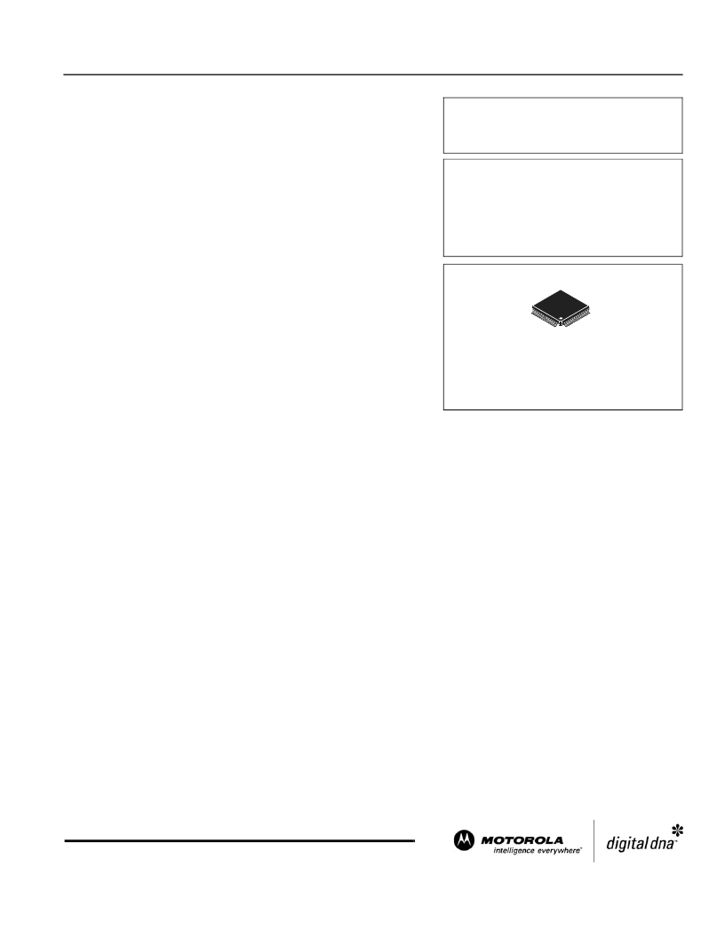
MPC9772
FA SUFFIX
52 LEAD LQFP PACKAGE
CASE 848D
3.3V 1:12 LVCMOS
PLL CLOCK GENERATOR
相關PDF資料 |
PDF描述 |
|---|---|
| MPC9893 | Low Voltage PLL Intelligent Dynamic Clock (IDCS) Switch |
| MPC99J93 | Intelligent Dynamic Clock Switch (IDCS) PLL Clock Driver |
| MPD-425V | 250W DC-DC POWER SUPPLY INPUT RANGE: 40~57VDC |
| MPE-902M | SWITCHING POWER SUPPLY |
| MPF102G | JFET VHF Amplifier |
相關代理商/技術參數 |
參數描述 |
|---|---|
| MPC9772AE | 功能描述:鎖相環 - PLL 2.5 3.3V 250MHz Clock Generator RoHS:否 制造商:Silicon Labs 類型:PLL Clock Multiplier 電路數量:1 最大輸入頻率:710 MHz 最小輸入頻率:0.002 MHz 輸出頻率范圍:0.002 MHz to 808 MHz 電源電壓-最大:3.63 V 電源電壓-最小:1.71 V 最大工作溫度:+ 85 C 最小工作溫度:- 40 C 封裝 / 箱體:QFN-36 封裝:Tray |
| MPC9772AER2 | 功能描述:時鐘發生器及支持產品 FSL 1-12 LVCMOS PLL Clock Generator, xta RoHS:否 制造商:Silicon Labs 類型:Clock Generators 最大輸入頻率:14.318 MHz 最大輸出頻率:166 MHz 輸出端數量:16 占空比 - 最大:55 % 工作電源電壓:3.3 V 工作電源電流:1 mA 最大工作溫度:+ 85 C 安裝風格:SMD/SMT 封裝 / 箱體:QFN-56 |
| MPC9772FA | 功能描述:鎖相環 - PLL 3.3V 240MHz Clock Generator RoHS:否 制造商:Silicon Labs 類型:PLL Clock Multiplier 電路數量:1 最大輸入頻率:710 MHz 最小輸入頻率:0.002 MHz 輸出頻率范圍:0.002 MHz to 808 MHz 電源電壓-最大:3.63 V 電源電壓-最小:1.71 V 最大工作溫度:+ 85 C 最小工作溫度:- 40 C 封裝 / 箱體:QFN-36 封裝:Tray |
| MPC9772FAR2 | 功能描述:時鐘發生器及支持產品 FSL 1-12 LVCMOS PLL Clock Generator, xta RoHS:否 制造商:Silicon Labs 類型:Clock Generators 最大輸入頻率:14.318 MHz 最大輸出頻率:166 MHz 輸出端數量:16 占空比 - 最大:55 % 工作電源電壓:3.3 V 工作電源電流:1 mA 最大工作溫度:+ 85 C 安裝風格:SMD/SMT 封裝 / 箱體:QFN-56 |
| MPC9773 | 制造商:FREESCALE 制造商全稱:Freescale Semiconductor, Inc 功能描述:3.3 V 1:12 LVCMOS PLL Clock Generator |
發布緊急采購,3分鐘左右您將得到回復。