- 您現在的位置:買賣IC網 > PDF目錄382345 > MPC9893 (Motorola, Inc.) Low Voltage PLL Intelligent Dynamic Clock (IDCS) Switch PDF資料下載
參數資料
| 型號: | MPC9893 |
| 廠商: | Motorola, Inc. |
| 英文描述: | Low Voltage PLL Intelligent Dynamic Clock (IDCS) Switch |
| 中文描述: | 低壓智能動態時鐘鎖相環(IDC機房)開關 |
| 文件頁數: | 1/16頁 |
| 文件大小: | 475K |
| 代理商: | MPC9893 |
MOTOROLA
SEMICONDUCTOR TECHNICAL DATA
Document Number: MPC9893/D
Rev 3, 01/2004
Motorola, Inc. 2004
Low Voltage PLL Intelligent
Dynamic Clock (IDCS) Switch
The MPC9893 is a 2.5V and 3.3V compatible, PLL based intelligent
dynamic clock switch and generator specifically designed for redundant
clock distribution systems. The device receives two LVCMOS clock
signals and generates 12 phase aligned output clocks. The MPC9893 is
able to detect a failing reference clock signal and to dynamically switch to
a redundant clock signal. The switch from the failing clock to the
redundant clock occurs without interruption of the output clock signal
(output clock slews to alignment). The phase bump typically caused by a
clock failure is eliminated.
The device offers 12 low skew clock outputs organized into two output
banks, each configurable to support the different clock frequencies.
The extended temperature range of the MPC9893 supports
telecommunication and networking requirements. The device employs a
fully differential PLL design to minimize jitter.
Features
12 output LVCMOS PLL clock generator
2.5V and 3.3V compatible
IDCS - on-chip intelligent dynamic clock switch
Automatically detects clock failure
Smooth output phase transition during clock failover switch
7.5 - 200 MHz output frequency range
LVCMOS compatible inputs and outputs
External feedback enables zero-delay configurations
Supports networking, telecommunications and computer applications
Output enable/disable and static test mode (PLL bypass)
Low skew characteristics: maximum 50 ps output-to-output (within bank)
48 lead LQFP package
Ambient operating temperature range of --40 to 85
°
C
Functional Description
The MPC9893 is a 3.3V or 2.5V compatible PLL clock driver and clock generator. The clock generator uses a fully integrated
PLL to generate clock signals from redundant clock sources. The PLL multiplies the input reference clock signal by one, two,
three, four or eight. The frequency-multiplied clock drives six bank A outputs. Six bank B outputs can run at either the same
frequency than bank A or at half of the bank A frequency. Therefore, bank B outputs additionally support the frequency
multiplication of the input reference clock by 3
÷
2 and 1
÷
2. Bank A and bank B outputs are phase-aligned
1
. Due to the external
PLL feedback, the clock signals of both output banks are also phase-aligned
1
to the selected input reference clock, providing
virtually zero-delay capability. The integrated IDCS continuously monitors both clock inputs and indicates a clock failure
individually for each clock input. When a false clock signal is detected, the MPC9893 switches to the redundant clock input,
forcing the PLL to slowly slew to alignment and not produce any phase bumps at the outputs. Both clock inputs are
interchangeable, also supporting the switch to a failed clock that was restored. The MPC9893 also provides a manual mode that
allows for user-controlled clock switches.
The PLL bypass of the MPC9893 disables the IDCS and PLL-related specifications do not apply. In PLL bypass mode, the
MPC9893 is fully static in order to distribute low-frequency clocks for system test and diagnosis. Outputs of the MPC9893 can be
disabled (high-impedance tristate) to isolate the device from the system. Applying output disable also resets the MPC9893. On
power-up this reset function needs to be applied for correct operation of the circuitry. Please see the application section for
power-on sequence recommendations.
The device is packaged in a 7x7 mm
2
48-lead LQFP package.
1. At coincident rising edges
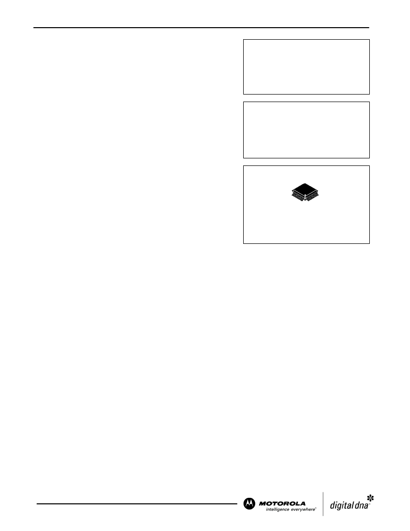
MPC9893
LOW VOLTAGE 2.5V AND 3.3V
IDCS AND PLL
CLOCK GENERATOR
FA SUFFIX
48--LEAD LQFP PACKAGE
CASE 932
F
Freescale Semiconductor, Inc.
For More Information On This Product,
Go to: www.freescale.com
n
.
相關PDF資料 |
PDF描述 |
|---|---|
| MPC99J93 | Intelligent Dynamic Clock Switch (IDCS) PLL Clock Driver |
| MPD-425V | 250W DC-DC POWER SUPPLY INPUT RANGE: 40~57VDC |
| MPE-902M | SWITCHING POWER SUPPLY |
| MPF102G | JFET VHF Amplifier |
| MPF4392G | JFET Switching Transistors N−Channel − Depletion |
相關代理商/技術參數 |
參數描述 |
|---|---|
| MPC9893AE | 功能描述:時鐘發生器及支持產品 RoHS:否 制造商:Silicon Labs 類型:Clock Generators 最大輸入頻率:14.318 MHz 最大輸出頻率:166 MHz 輸出端數量:16 占空比 - 最大:55 % 工作電源電壓:3.3 V 工作電源電流:1 mA 最大工作溫度:+ 85 C 安裝風格:SMD/SMT 封裝 / 箱體:QFN-56 |
| MPC9893AER2 | 功能描述:時鐘發生器及支持產品 RoHS:否 制造商:Silicon Labs 類型:Clock Generators 最大輸入頻率:14.318 MHz 最大輸出頻率:166 MHz 輸出端數量:16 占空比 - 最大:55 % 工作電源電壓:3.3 V 工作電源電流:1 mA 最大工作溫度:+ 85 C 安裝風格:SMD/SMT 封裝 / 箱體:QFN-56 |
| MPC9893FA | 功能描述:時鐘發生器及支持產品 2.5 3.3V 200MHz Clock Generator RoHS:否 制造商:Silicon Labs 類型:Clock Generators 最大輸入頻率:14.318 MHz 最大輸出頻率:166 MHz 輸出端數量:16 占空比 - 最大:55 % 工作電源電壓:3.3 V 工作電源電流:1 mA 最大工作溫度:+ 85 C 安裝風格:SMD/SMT 封裝 / 箱體:QFN-56 |
| MPC9893FAR2 | 制造商:Integrated Device Technology Inc 功能描述:PLL Clock Driver Single 48-Pin LQFP T/R 制造商:Integrated Device Technology Inc 功能描述:MPC9893FAR2 - Tape and Reel |
| MPC9894 | 制造商:未知廠家 制造商全稱:未知廠家 功能描述:Quad Input Redundant IDCS Clock Generator |
發布緊急采購,3分鐘左右您將得到回復。