- 您現在的位置:買賣IC網 > Datasheet目錄45 > NCP1603D100R2G (ON Semiconductor)IC CTLR PFC/PWM COMBO 16-SOIC Datasheet資料下載
參數資料
| 型號: | NCP1603D100R2G |
| 廠商: | ON Semiconductor |
| 文件頁數: | 16/30頁 |
| 文件大小: | 302K |
| 描述: | IC CTLR PFC/PWM COMBO 16-SOIC |
| 產品變化通告: | Product Discontinuation 21/Jun/2007 |
| 標準包裝: | 2,500 |
| 模式: | 臨界傳導(CRM),間歇導電(DCM) |
| 頻率 - 開關: | 58kHz |
| 電流 - 啟動: | 17µA |
| 電源電壓: | 9 V ~ 18 V |
| 工作溫度: | -40°C ~ 125°C |
| 安裝類型: | 表面貼裝 |
| 封裝/外殼: | 16-SOIC(0.154",3.90mm 寬) |
| 供應商設備封裝: | 16-SOIC |
| 包裝: | 帶卷 (TR) |
第1頁第2頁第3頁第4頁第5頁第6頁第7頁第8頁第9頁第10頁第11頁第12頁第13頁第14頁第15頁當前第16頁第17頁第18頁第19頁第20頁第21頁第22頁第23頁第24頁第25頁第26頁第27頁第28頁第29頁第30頁
NCP1603
http://onsemi.com
16
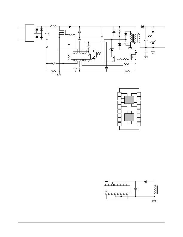
OPERATING DESCRIPTION
Figure 45. Typical Application Circuit
EMI
Filter
NCP1603
+
V
ac
Z
OVP
V
out
V
in
L
I
L
D
1
C
filter
Q
1
R
S1
R
CS1
C
bulk
C
osc
R
FB1
I
FB1
I
S
C
control
C
ramp
R
CS2
R
S2
V
bulk
R
FF
I
D
D
3
Q
2
D
2
C
out
C
s
Z
ref
Introduction
The NCP1603 is a PWM/PFC combo controller for
twostages PFC lowpower application. A typical
application circuit is listed in Figure 45. The firststage PFC
boost circuit draws a nearunity power factor current from the
input but it also steps up the rectified input voltage V
in
to a
high bulk voltage V
bulk
in the bulk capacitor C
bulk
. Then, the
secondstage PWM flyback circuit converts the bulk voltage
V
bulk
to a usable low voltage and isolated output voltage V
out
.
The controllers of the two stages are combined to become a
single PWM/PFC combo controller. The advantages of
NCP1603 are the following:
1. Integrated maximum 500 V lossless high voltage
startup circuit that saves area and power loss.
2. Low standby power consumption because of PFC
shutdown and skipping cycle operation.
3. Proprietary PFC methodology limits the
maximum switching frequency and frequency
jittering feature of the secondstage make the
easier frontended EMI filter design.
4. Internal ramp compensation for stability
improvement in the second stage converter.
5. Minimum number of external components.
6. Optional synchronization capability between the
PFC and PWM sections for bulk capacitor ripple
current reduction.
7. Safety protection features.
NCP1603 is a copackage of two individual IC dies.
(NCP1601 and NCP1230, 100 kHz) The PFC die links up
pin 5 to pin 12 that are in the lower half of Figure 46. The
PWM die links up the other pins that are in the upper half
of Figure 46. For simplicity, the PFC pins are named with
suffix one that stands for the first stage and the PWM pins
are named with suffix two that stands for the second stage.
This dualdies architecture allows the PFC die to be
completely powered off in the standby lowpower
condition. It makes the power supply an excellent
lowpower no load standby performance.
16
15
14
12
11
10
9
HV
NC
Ramp
CS1
FB1
V
CC2
V
control
13 Out2
1
2
3
4
5
6
7
8
Osc
FB2
CS2
GND2
GND1
Out1
V
CC1
V
aux
PWM
Die
PFC
Die
Figure 46. Internal Connection
Biasing the Controller
The PWM section is the master section that always
operates. The PFC section is the slave section that is
powered off in standby condition for power saving. It is
implemented by connecting V
aux
pin (Pin 1) and V
CC1
pin
(Pin 8) together externally. The V
CC1
pin generally
requires a small decoupling external capacitor (0.1 mF) or
nothing. The PWM section powers the PFC section. The
V
CC
of the whole device refers to V
CC2
(Pin 14) in the
PWM section (i.e., V
CC
= V
CC2
).
Figure 47. Bias Supply Schematic
NCP1603
16
14
1
4
6
8
V
bulk
V
CC2
C
VCC
GND1 = GND2
V
CC1
= V
aux
相關PDF資料 |
PDF描述 |
|---|---|
| NCP1605DR2G | IC PFC CONTROLLER CCM/DCM 16SOIC |
| NCP1606BDR2G | IC POWER FACTOR CONTROLLER 8SOIC |
| NCP1607BDR2G | IC PFC CONTROLLER CRM 8SOIC |
| NCP1611BDR2G | IC PFC CTLR HE ENHANCED 8-SOIC |
| NCP1651DR2G | IC PFC CONTROLLER CCM/DCM 16SOIC |
相關代理商/技術參數 |
參數描述 |
|---|---|
| NCP1605ADR2G | 功能描述:功率因數校正 IC ENHANCED PFC CNTRLER RoHS:否 制造商:Fairchild Semiconductor 開關頻率:300 KHz 最大功率耗散: 最大工作溫度:+ 125 C 安裝風格:SMD/SMT 封裝 / 箱體:SOIC-8 封裝:Reel |
| NCP1605BDR2G | 功能描述:功率因數校正 IC High Volt Stby Mode Power Fact Corr Cont RoHS:否 制造商:Fairchild Semiconductor 開關頻率:300 KHz 最大功率耗散: 最大工作溫度:+ 125 C 安裝風格:SMD/SMT 封裝 / 箱體:SOIC-8 封裝:Reel |
| NCP1605DR2G | 功能描述:功率因數校正 IC Enhanced PFC HV and Eff Standby RoHS:否 制造商:Fairchild Semiconductor 開關頻率:300 KHz 最大功率耗散: 最大工作溫度:+ 125 C 安裝風格:SMD/SMT 封裝 / 箱體:SOIC-8 封裝:Reel |
| NCP1605FORWGEVB | 功能描述:電源管理IC開發工具 NCP1605 152 W FORWARD EVB RoHS:否 制造商:Maxim Integrated 產品:Evaluation Kits 類型:Battery Management 工具用于評估:MAX17710GB 輸入電壓: 輸出電壓:1.8 V |
| NCP1605LCDTVGEVB | 功能描述:BOARD EVAL NCP1605/1396 RoHS:是 類別:編程器,開發系統 >> 評估演示板和套件 系列:* 產品培訓模塊:Obsolescence Mitigation Program 標準包裝:1 系列:- 主要目的:電源管理,電池充電器 嵌入式:否 已用 IC / 零件:MAX8903A 主要屬性:1 芯鋰離子電池 次要屬性:狀態 LED 已供物品:板 |
發布緊急采購,3分鐘左右您將得到回復。