- 您現在的位置:買賣IC網 > Datasheet目錄45 > NCP1603D100R2G (ON Semiconductor)IC CTLR PFC/PWM COMBO 16-SOIC Datasheet資料下載
參數資料
| 型號: | NCP1603D100R2G |
| 廠商: | ON Semiconductor |
| 文件頁數: | 26/30頁 |
| 文件大小: | 302K |
| 描述: | IC CTLR PFC/PWM COMBO 16-SOIC |
| 產品變化通告: | Product Discontinuation 21/Jun/2007 |
| 標準包裝: | 2,500 |
| 模式: | 臨界傳導(CRM),間歇導電(DCM) |
| 頻率 - 開關: | 58kHz |
| 電流 - 啟動: | 17µA |
| 電源電壓: | 9 V ~ 18 V |
| 工作溫度: | -40°C ~ 125°C |
| 安裝類型: | 表面貼裝 |
| 封裝/外殼: | 16-SOIC(0.154",3.90mm 寬) |
| 供應商設備封裝: | 16-SOIC |
| 包裝: | 帶卷 (TR) |
第1頁第2頁第3頁第4頁第5頁第6頁第7頁第8頁第9頁第10頁第11頁第12頁第13頁第14頁第15頁第16頁第17頁第18頁第19頁第20頁第21頁第22頁第23頁第24頁第25頁當前第26頁第27頁第28頁第29頁第30頁
NCP1603
http://onsemi.com
26
The PFC section is designed to operate in either DCM or
CRM. In order to keep the operation in DCM and CRM
only, the Drive Output cannot turn on as long as there is
some inductor current flowing through the circuit. Hence,
the zero current signal is provided to the oscillator/
synchronization block in Figure 67. An input comparator
monitors the Osc pin (Pin 5) voltage and generates a clock
signal. The negative edge of the clock signal is stored in a
RS latch. When zero current is detected, the RS latch will
be reset and a set signal is sent to the output drive latch that
turns on the MOSFET in the PFC boost circuit. Figure 68
illustrates a typical timing diagram of the oscillator block.
Figure 68. Oscillator Block Timing Diagram
time
clock
inductor
clock latch
(latch set signal)
Discontinuous mode
Critical mode
(latch output)
current
clock edge
Oscillator Mode in PFC Section
In oscillator mode, the Osc pin (Pin 5) is connected to an
external capacitor C
osc
. When the voltage of this pin is above
V
sync(H)
(5.0 V typical), the pin sinks a current I
odch
(9445
= 49 mA typical) and the external capacitor C
osc
discharges.
When the voltage reaches V
sync(L)
(3.5 V typical), the pin
sources a current I
och
(45 mA typical) and the external
capacitor C
osc
is charged. It is noted that there is a typical
300 ns propagation delay and the 3.5 V and 5.0 V threshold
conditions are measured on 220 pF C
osc
capacitor. Hence, the
actual oscillator hysteresis is a little bit smaller.
Figure 69. Oscillator Mode Timing Diagram in DCM
Osc pin
voltage
Osc clock
Clock edge
Drive output
(DCM)
5 V
3.5 V
There is an internal capacitance C
osc(int)
(36 pF typical)
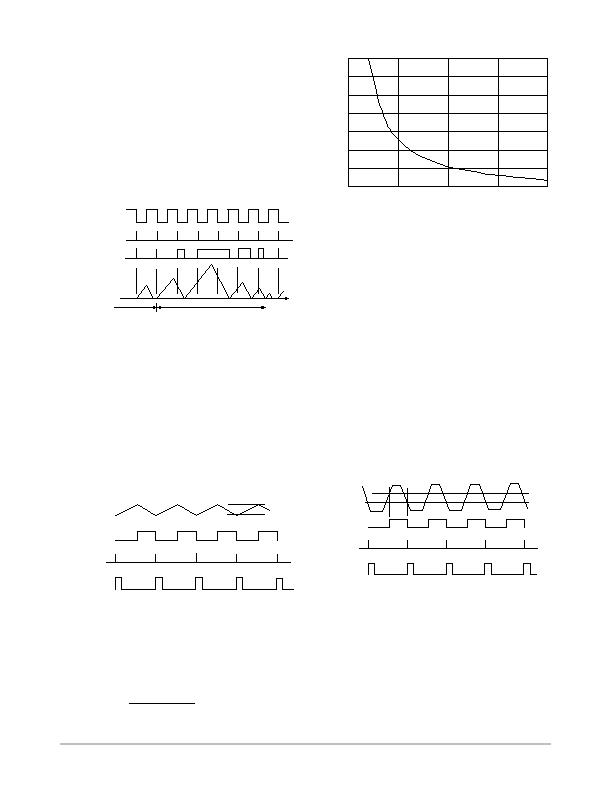
in the oscillator pin and the oscillator frequency is to
f
osc(max)
(405 kHz typical) when the Osc pin is opened.
Hence, the oscillator switching frequency can be
formulated in Equation 25 and represented in Figure 70.
C
osc
+
36 pF @ 405 kHz
f
osc
* 36 pF
(eq. 25)
0
100
200
300
400
500
600
700
0
50
100
150
200
f
osc
, Oscillator Frequency (kHz)
Figure 70. Osc Pin Frequency Setting
Synchronization Option
In synchronization mode, the Osc pin (Pin 5) receives an
external digital signal with level high defined to be higher
than V
sync(H)
(5.0 V typical) and level low defined to be
lower than V
sync(L)
(3.5 V typical). An internal 9.0 V ESD
Zener diode is connected to the Osc pin and hence the
maximum allowable synchronization voltage is 9.0 V. The
circuit recognizes a synchronization frequency by the time
difference between two falling edge instants when the
synchronization signal across the 3.5 V threshold point.
The actual synchronization threshold point is a little bit
higher than the 3.5 V threshold point. The minimum
synchronization pulse width is 500 ns.
There is a typical 350 ns propagation delay from
synchronization threshold point to the moment of output goes
high and there is also a typical 300 ns propagation delay from
the synchronization threshold point to the moment of crossing
3.5 V. Hence, the output goes high apparently when the sync
signal turns to 3.5 V. A timing diagram of synchronization
mode is summarized in Figure 71.
Figure 71. Synchronization Mode Timing Diagram in
DCM
Sync Signal
Osc Clock
Clock Edge
Drive Output
(DCM)
5 V
3.5 V
The PWM and PFC Section can be synchronized
together in order to minimize some of the ripple current in
the bulk capacitor as shown in Figure 72 and 73. The Out2
pin (Pin 13) is the external synchronization signal in
Figure 71 to the PFC Section. When the Out2 is in high
state, the voltage is potentially higher than the maximum
allowable voltage in Osc pin (Pin 5). Hence, a pair of
resistors divides the voltage from Out2 reduces the voltage
相關PDF資料 |
PDF描述 |
|---|---|
| NCP1605DR2G | IC PFC CONTROLLER CCM/DCM 16SOIC |
| NCP1606BDR2G | IC POWER FACTOR CONTROLLER 8SOIC |
| NCP1607BDR2G | IC PFC CONTROLLER CRM 8SOIC |
| NCP1611BDR2G | IC PFC CTLR HE ENHANCED 8-SOIC |
| NCP1651DR2G | IC PFC CONTROLLER CCM/DCM 16SOIC |
相關代理商/技術參數 |
參數描述 |
|---|---|
| NCP1605ADR2G | 功能描述:功率因數校正 IC ENHANCED PFC CNTRLER RoHS:否 制造商:Fairchild Semiconductor 開關頻率:300 KHz 最大功率耗散: 最大工作溫度:+ 125 C 安裝風格:SMD/SMT 封裝 / 箱體:SOIC-8 封裝:Reel |
| NCP1605BDR2G | 功能描述:功率因數校正 IC High Volt Stby Mode Power Fact Corr Cont RoHS:否 制造商:Fairchild Semiconductor 開關頻率:300 KHz 最大功率耗散: 最大工作溫度:+ 125 C 安裝風格:SMD/SMT 封裝 / 箱體:SOIC-8 封裝:Reel |
| NCP1605DR2G | 功能描述:功率因數校正 IC Enhanced PFC HV and Eff Standby RoHS:否 制造商:Fairchild Semiconductor 開關頻率:300 KHz 最大功率耗散: 最大工作溫度:+ 125 C 安裝風格:SMD/SMT 封裝 / 箱體:SOIC-8 封裝:Reel |
| NCP1605FORWGEVB | 功能描述:電源管理IC開發工具 NCP1605 152 W FORWARD EVB RoHS:否 制造商:Maxim Integrated 產品:Evaluation Kits 類型:Battery Management 工具用于評估:MAX17710GB 輸入電壓: 輸出電壓:1.8 V |
| NCP1605LCDTVGEVB | 功能描述:BOARD EVAL NCP1605/1396 RoHS:是 類別:編程器,開發系統 >> 評估演示板和套件 系列:* 產品培訓模塊:Obsolescence Mitigation Program 標準包裝:1 系列:- 主要目的:電源管理,電池充電器 嵌入式:否 已用 IC / 零件:MAX8903A 主要屬性:1 芯鋰離子電池 次要屬性:狀態 LED 已供物品:板 |
發布緊急采購,3分鐘左右您將得到回復。