- 您現在的位置:買賣IC網 > Datasheet目錄45 > NCP1603D100R2G (ON Semiconductor)IC CTLR PFC/PWM COMBO 16-SOIC Datasheet資料下載
參數資料
| 型號: | NCP1603D100R2G |
| 廠商: | ON Semiconductor |
| 文件頁數: | 23/30頁 |
| 文件大小: | 302K |
| 描述: | IC CTLR PFC/PWM COMBO 16-SOIC |
| 產品變化通告: | Product Discontinuation 21/Jun/2007 |
| 標準包裝: | 2,500 |
| 模式: | 臨界傳導(CRM),間歇導電(DCM) |
| 頻率 - 開關: | 58kHz |
| 電流 - 啟動: | 17µA |
| 電源電壓: | 9 V ~ 18 V |
| 工作溫度: | -40°C ~ 125°C |
| 安裝類型: | 表面貼裝 |
| 封裝/外殼: | 16-SOIC(0.154",3.90mm 寬) |
| 供應商設備封裝: | 16-SOIC |
| 包裝: | 帶卷 (TR) |
第1頁第2頁第3頁第4頁第5頁第6頁第7頁第8頁第9頁第10頁第11頁第12頁第13頁第14頁第15頁第16頁第17頁第18頁第19頁第20頁第21頁第22頁當前第23頁第24頁第25頁第26頁第27頁第28頁第29頁第30頁
NCP1603
http://onsemi.com
23
a 9.0 V ESD zener diode. The 3.9 V maximum limit of this
V
ton
indirectly limits the maximum on time.
The V
control
processing circuit generates V
ton
from
control voltage V
control
and time information of zero
inductor current. The circuit in Figure 61 makes
Equations 9 and 10 where the value of resistor R
1
is much
higher than the value of resistor R
2
(R
1
>> R
2
).
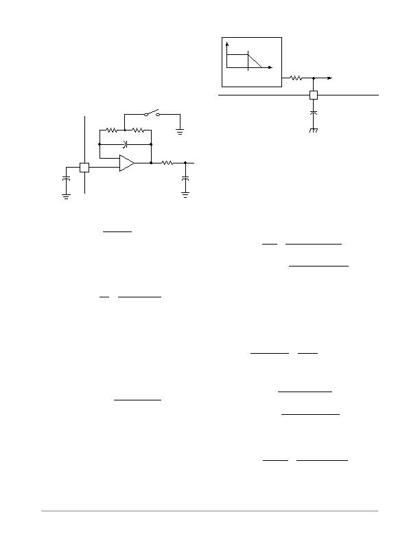
Figure 61. V
control
Processing Circuit
+
closed when zero current
10
C
control
V
control
R
1
R
2
R
3
C
1
C
3
V
ton
V
ton
+
T V
control
t
1
) t
2
for DCM
(eq. 9)
V
ton
+ V
control
for CRM
(eq. 10)
It is noted that V
ton
is always greater than or equal to
V
control
(V
ton
q V
control
).
In summary, the input impedance Z
in
in Equation 11 is
obtained from Equations 3 through 10.
Z
in
+
V
in
I
in
+
2LI
ch
C
ramp
V
control
(eq. 11)
Control voltage V
control
comes from the PFC boost
circuit output voltage (i.e., bulk voltage V
bulk
) that is a
slowly varying signal. The bandwidth of V
control
can be
additionally limited by inserting an external capacitor
C
control
to the V
control
pin (Pin 10) in Figure 62. The
internal 300 kW resistor and the capacitor C
control
create a
lowpass filter that has a bandwidth f
control
in Equation 12.
It is generally recommended to limit the bandwidth below
20 Hz to achieve power factor correction. Typical value of
C
control
is 0.1 mF.
C
control
u
1
2p300kW f
control
(eq. 12)
Figure 62. V
control
LowPass Filtering
300k
Regulation Block
10
C
control
V
control
V
reg
I
ref
I
ref
96%
I
FB1
V
control
Processing
Circuit
If the bandwidth of V
control
is much less than the 50 or
60 Hz line frequency, the input impedance Z
in
is slowly
varying or roughly constant. Then, the power factor
correction is achieved in DCM and CRM.
Maximum Power in PFC Section
Input and output power (P
in
and P
out
) are derived in
Equations 13 and 14 when the circuit efficiency ? is
obtained or assumed. The variable V
ac
stands for the RMS
input voltage.
P
in
+
V
ac
2
Z
in
+
V
ac
2
C
ramp
V
control
2LI
ch
(eq. 13)
P
out
+ h P
in
+
hV
ac
2
C
ramp
V
control
2LI
ch
(eq. 14)
From Equations 13 and 14, control voltage V
control
controls the amount of output power, input power, or input
impedance. The maximum value of the control voltage
V
control
is 1.05 V (i.e., V
control(max)
= 1.05 V). A parameter
called maximum power resistor R
power
(10.5 kW typical) is
defined in Equation 18 and restricted to have a maximum
?0% variation (i.e., 9.5 kW p R
power
p 11.5 kW) for
defining the maximum power in an application.
R
power
+
V
control(max)
I
ch
+
1.05 V
100 mA
+ 10.5 kW
(eq. 15)
It means that the maximum input and output power
(P
in(max)
and P
out(max)
) are limited to ?0% variation.
P
in(max)
+
V
ac
2
C
ramp
R
power
2 L
(eq. 16)
P
out(max)
+
hV
ac
2
C
ramp
R
power
2 L
(eq. 17)
The maximum input current I
ac(max)
to deliver the
maximum input power P
in(max)
is also derived in (eq.14).
The suffix ac stands for RMS value.
I
ac(max)
+
P
in(max)
V
ac
+
V
acC
ramp
R
power
2 L
(eq. 18)
相關PDF資料 |
PDF描述 |
|---|---|
| NCP1605DR2G | IC PFC CONTROLLER CCM/DCM 16SOIC |
| NCP1606BDR2G | IC POWER FACTOR CONTROLLER 8SOIC |
| NCP1607BDR2G | IC PFC CONTROLLER CRM 8SOIC |
| NCP1611BDR2G | IC PFC CTLR HE ENHANCED 8-SOIC |
| NCP1651DR2G | IC PFC CONTROLLER CCM/DCM 16SOIC |
相關代理商/技術參數 |
參數描述 |
|---|---|
| NCP1605ADR2G | 功能描述:功率因數校正 IC ENHANCED PFC CNTRLER RoHS:否 制造商:Fairchild Semiconductor 開關頻率:300 KHz 最大功率耗散: 最大工作溫度:+ 125 C 安裝風格:SMD/SMT 封裝 / 箱體:SOIC-8 封裝:Reel |
| NCP1605BDR2G | 功能描述:功率因數校正 IC High Volt Stby Mode Power Fact Corr Cont RoHS:否 制造商:Fairchild Semiconductor 開關頻率:300 KHz 最大功率耗散: 最大工作溫度:+ 125 C 安裝風格:SMD/SMT 封裝 / 箱體:SOIC-8 封裝:Reel |
| NCP1605DR2G | 功能描述:功率因數校正 IC Enhanced PFC HV and Eff Standby RoHS:否 制造商:Fairchild Semiconductor 開關頻率:300 KHz 最大功率耗散: 最大工作溫度:+ 125 C 安裝風格:SMD/SMT 封裝 / 箱體:SOIC-8 封裝:Reel |
| NCP1605FORWGEVB | 功能描述:電源管理IC開發工具 NCP1605 152 W FORWARD EVB RoHS:否 制造商:Maxim Integrated 產品:Evaluation Kits 類型:Battery Management 工具用于評估:MAX17710GB 輸入電壓: 輸出電壓:1.8 V |
| NCP1605LCDTVGEVB | 功能描述:BOARD EVAL NCP1605/1396 RoHS:是 類別:編程器,開發系統 >> 評估演示板和套件 系列:* 產品培訓模塊:Obsolescence Mitigation Program 標準包裝:1 系列:- 主要目的:電源管理,電池充電器 嵌入式:否 已用 IC / 零件:MAX8903A 主要屬性:1 芯鋰離子電池 次要屬性:狀態 LED 已供物品:板 |
發布緊急采購,3分鐘左右您將得到回復。