- 您現在的位置:買賣IC網 > PDF目錄382385 > PCT1789N PCT303DL PDF資料下載
參數資料
| 型號: | PCT1789N |
| 英文描述: | PCT303DL |
| 中文描述: | PCT303DL |
| 文件頁數: | 33/40頁 |
| 文件大小: | 632K |
| 代理商: | PCT1789N |
第1頁第2頁第3頁第4頁第5頁第6頁第7頁第8頁第9頁第10頁第11頁第12頁第13頁第14頁第15頁第16頁第17頁第18頁第19頁第20頁第21頁第22頁第23頁第24頁第25頁第26頁第27頁第28頁第29頁第30頁第31頁第32頁當前第33頁第34頁第35頁第36頁第37頁第38頁第39頁第40頁
PC-TEL, Inc.
56
1789N0DOCDAT01A-0399
PCT1789N DATA SHEET
S
WITCHING
C
HARACTERISTICS
!
PRELIMINARY
PRELIMINARY
Serial Interface (DCE = 0)
Given values are: V
A
= charge pump, V
D
= 3.0 V to 5.25 V; T
A
= 0 °C to 70 °C for K-grade, –40 °C to +85 °C for
B-grade; C
L
= 20 pF.
All timing is referenced to the 50% level of the waveform. Input test levels are: V
IH
= V
D
– 0.4V, V
IL
= 0.4V.
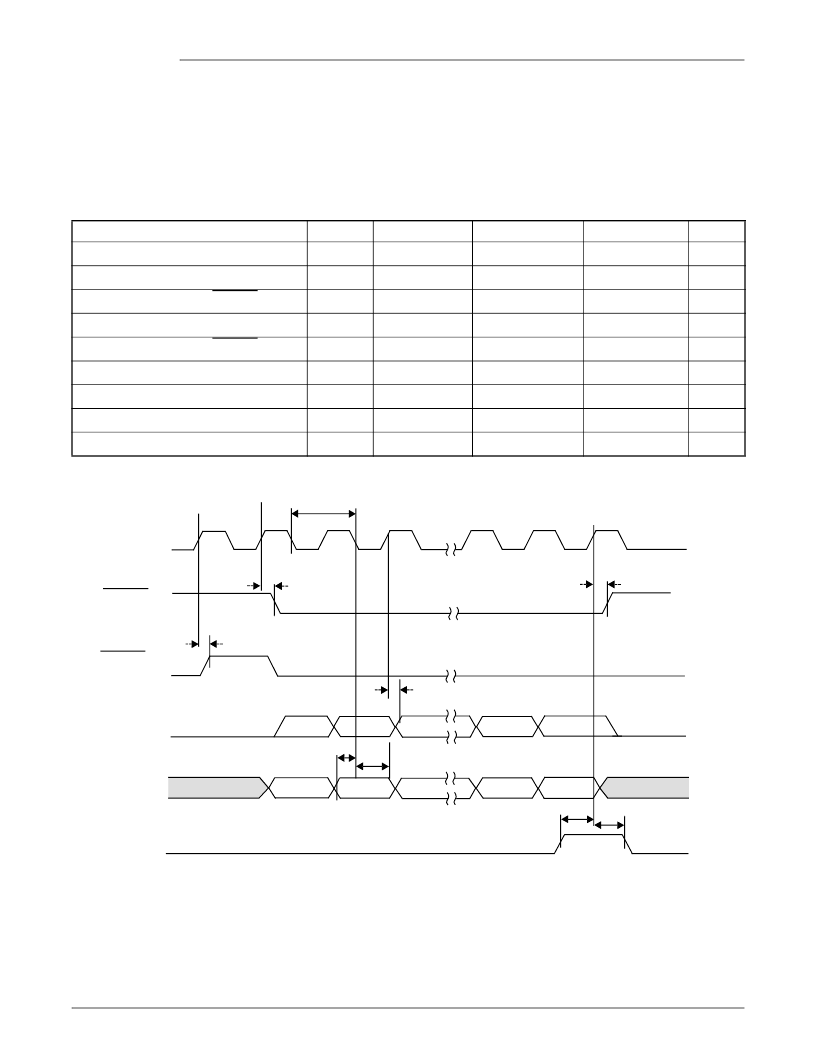
Table 24 Switching Characteristics—Serial Interface (DCE = 0)
Figure 19 Serial Interface Timing Diagram (DCE = 0)
Parameter
Cycle time, SCLK
Symbol
t
c
t
dty
t
d1
t
d2
t
d3
t
su
t
h
t
sfc
t
hfc
Min
354
Typ
Max
Unit
ns
1/256 Fs
SCLK duty cycle
50
%
Delay time, SCLK
↑
to FSYNC
↓
Delay time, SCLK
↑
to SDO valid
Delay time, SCLK
↑
to FSYNC
↑
Setup time, SDI before SCLK
↓
Hold time, SDI after SCLK
↓
Setup time, FC
↑
before SCLK
↑
Hold time, FC
↑
after SCLK
↑
–10
20
ns
20
ns
–10
20
ns
25
ns
20
ns
40
ns
40
ns
SCLK
V
OH
V
OL
D15
D14
D1
D0
16-bit
SDO
D15
D14
D1
D0
16-bit
SDI
t
d2
t
su
t
h
FSYNC
(mode 1)
t
d3
t
c
t
hfc
t
sfc
FC
FSYNC
(mode 0)
t
d1
t
d3
相關PDF資料 |
PDF描述 |
|---|---|
| PCV250TWG5 | |
| PCV250TWLY5 | |
| PCV250TWO5 | |
| PCV250TWPG5 | |
| PCV250TWR5 | |
相關代理商/技術參數 |
參數描述 |
|---|---|
| PCT-178F-Q | 制造商:Panduit Corp 功能描述: |
| PCT-179F-Q | 制造商:Panduit Corp 功能描述:Call vendor for pricing |
| PCT-18 | 制造商:Stancor 功能描述: |
| PCT-182F-Q | 制造商:Panduit Corp 功能描述: |
| PCT-1861 | 制造商:MICRO-ELECTRONICS 制造商全稱:Micro Electronics 功能描述:MODEM TRANSFORMER |
發布緊急采購,3分鐘左右您將得到回復。