- 您現(xiàn)在的位置:買賣IC網(wǎng) > PDF目錄98215 > TFP403PZPG4 (TEXAS INSTRUMENTS INC) SPECIALTY CONSUMER CIRCUIT, PQFP100 PDF資料下載
參數(shù)資料
| 型號(hào): | TFP403PZPG4 |
| 廠商: | TEXAS INSTRUMENTS INC |
| 元件分類: | 消費(fèi)家電 |
| 英文描述: | SPECIALTY CONSUMER CIRCUIT, PQFP100 |
| 封裝: | 14 X 14 MM, 1 MM HEIGHT, 0.50 MM PITCH, GREEN, PLASTIC, HTQFP-100 |
| 文件頁(yè)數(shù): | 15/20頁(yè) |
| 文件大小: | 496K |
| 代理商: | TFP403PZPG4 |
第1頁(yè)第2頁(yè)第3頁(yè)第4頁(yè)第5頁(yè)第6頁(yè)第7頁(yè)第8頁(yè)第9頁(yè)第10頁(yè)第11頁(yè)第12頁(yè)第13頁(yè)第14頁(yè)當(dāng)前第15頁(yè)第16頁(yè)第17頁(yè)第18頁(yè)第19頁(yè)第20頁(yè)
TFP403
TI PanelBus DIGITAL RECEIVER
SLDS125A DECEMBER 2000 REVISED OCTOBER 2002
4
POST OFFICE BOX 655303
DALLAS, TEXAS 75265
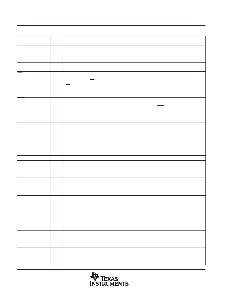
Terminal Functions (Continued)
TERMINAL
I/O
DESCRIPTION
NAME
NO.
I/O
DESCRIPTION
ODCK
44
DO
Output data clock—Pixel clock. All pixel outputs QE[23:0] and QO[23:0] (if in 2-pixel/clock mode) along with
DE, HSYNC, VSYNC, and CTL[2:1] are synchronized to this clock.
OGND
19,28,45,
58,76
GND
Output driver ground—Ground reference and current return for digital output drivers
OVDD
18,29,43,
57,78
VDD
Output driver VDD—Power supply for output drivers. Nominally 3.3 V
PD
2
DI
Power down—An active low signal that controls the TFP403 power-down state. During power down all output
buffers are switched to a high impedance state. All analog circuits are powered down and all inputs are
disabled, except for PD.
If PD is left unconnected an internal pullup will default the TFP403 to normal operation.
High : Normal operation
Low: Power down
PDO
9
DI
Output drive power down—An active low signal that controls the power-down state of the output drivers.
During output drive powerdown, the output drivers (except SCDT and CTL1) are driven to a high impedance
state. A weak pulldown will slowly pull these outputs to a low level. When PDO is left unconnected, an internal
pullup defaults the TFP403 to normal operation.
High : Normal operation/output drivers on
Low: Output drive power down.
PGND
98
GND
PLL GND—Ground reference and current return for internal PLL
PIXS
4
DI
Pixel select—Selects between one or two pixels per clock output modes. During the 2-pixel/clock mode, both
even pixels, QE[23:0], and odd pixels, QO[23:0], are output in tandem on a given clock cycle. During
1-pixel/clock, even and odd pixels are output sequentially, one at a time, with the even pixel first, on the even
pixel bus, QE[23:0]. (The first pixel per line is pixel-0, the even pixel. The second pixel per line is pixel-1, the
odd pixel.)
High : 2-pixel/clock
Low: 1-pixel/clock
PVDD
97
VDD
PLL VDD—Power supply for internal PLL. Nominally 3.3 V
QE[0:7]
10-17
DO
Even blue pixel output—Output for even and odd blue pixels when in 1-pixel/clock mode. Output for even only
blue pixel when in 2-pixel per clock mode. Output data is synchronized to the output data clock, ODCK.
LSB: QE0/pin 10
MSB: QE7/pin 17
QE[8:15]
20-27
DO
Even green pixel output—Output for even and odd green pixels when in 1-pixel/clock mode. Output for even
only green pixel when in 2-pixel/clock mode. Output data is synchronized to the output data clock, ODCK.
LSB: QE8/pin 20
MSB: QE15/pin 27
QE[16:23]
30-37
DO
Even red pixel output—Output for even and odd red pixels when in 1-pixel/clock mode. Output for even only
red pixel when in 2-pixel/clock mode. Output data is synchronized to the output data clock, ODCK.
LSB: QE16/pin 30
MSB: QE23/pin 37
QO[0:7]
49-56
DO
Odd blue pixel output—Output for odd only blue pixel when in 2-pixel/clock mode. Not used, and held low,
when in 1-pixel/clock mode. Output data is synchronized to the output data clock, ODCK.
LSB: QO0/pin 49
MSB: QO7/pin 56
QO[8:15]
59-66
DO
Odd green pixel output—Output for odd only green pixel when in 2-pixel/clock mode. Not used, and held low,
when in 1-pixel/clock mode. Output data is synchronized to the output data clock, ODCK.
LSB: QO8/pin 59
MSB: QO15/pin 66
QO[16:23]
69-75,77
DO
Odd red pixel output—Output for odd only red pixel when in 2-pixel/clock mode. Not used, and held low, when
in 1-pixel/clock mode. Output data is synchronized to the output data clock, ODCK.
LSB: QO16/pin 69
MSB: QO23/pin 77
相關(guān)PDF資料 |
PDF描述 |
|---|---|
| TFP420PAP | SPECIALTY CONSUMER CIRCUIT, PQFP64 |
| TFP501PZPG4 | SPECIALTY CONSUMER CIRCUIT, PQFP100 |
| TFP501PZP | SPECIALTY CONSUMER CIRCUIT, PQFP100 |
| TFP503PZPG4 | SPECIALTY CONSUMER CIRCUIT, PQFP100 |
| TFP503PZP | SPECIALTY CONSUMER CIRCUIT, PQFP100 |
相關(guān)代理商/技術(shù)參數(shù) |
參數(shù)描述 |
|---|---|
| TFP41 | 制造商:HOFFMAN ENCLOSURES 功能描述:COOLING FAN PACKAGE, 4 IN;115V 50/60HZ;; 制造商:Pentair Technical Products / Hoffman 功能描述:COOLING FAN 55CFM 15W 制造商:HOFFMAN ENCLOSURES 功能描述:COOLING FAN, 55CFM, 15W 制造商:Pentair Technical Products / Hoffman 功能描述:COOLING FAN, 55CFM, 15W; Enclosure Material:ABS; Body Color:Black; External Height - Imperial:6.29"; External Height - Metric:160mm; External Width - Imperial:7.37"; External Width - Metric:187mm; External Depth - Imperial:2.6" ;RoHS Compliant: Yes |
| TFP410 | 制造商:TI 制造商全稱:Texas Instruments 功能描述:TI PANEL BUS DIGITAL TRANSMITTER |
| TFP410-EP | 制造商:TI 制造商全稱:Texas Instruments 功能描述:PanelBusa?¢ DIGITAL TRANSMITTER |
| TFP410MPAPREP | 功能描述:顯示接口集成電路 PanelBus(TM) Digital Transmitter RoHS:否 制造商:Texas Instruments 電源電流:125 mA 工作溫度范圍:- 40 C to + 105 C 封裝 / 箱體:WQFN-60 封裝:Reel |
| TFP410MPAPREPG4 | 功能描述:顯示接口集成電路 EP Panelbus Dig Transmitter RoHS:否 制造商:Texas Instruments 電源電流:125 mA 工作溫度范圍:- 40 C to + 105 C 封裝 / 箱體:WQFN-60 封裝:Reel |
發(fā)布緊急采購(gòu),3分鐘左右您將得到回復(fù)。