- 您現(xiàn)在的位置:買賣IC網(wǎng) > PDF目錄98266 > TMDS442PNPRG4 (TEXAS INSTRUMENTS INC) SPECIALTY CONSUMER CIRCUIT, PQFP128 PDF資料下載
參數(shù)資料
| 型號(hào): | TMDS442PNPRG4 |
| 廠商: | TEXAS INSTRUMENTS INC |
| 元件分類: | 消費(fèi)家電 |
| 英文描述: | SPECIALTY CONSUMER CIRCUIT, PQFP128 |
| 封裝: | PLASTIC, TQFP-128 |
| 文件頁(yè)數(shù): | 21/45頁(yè) |
| 文件大小: | 1977K |
| 代理商: | TMDS442PNPRG4 |
第1頁(yè)第2頁(yè)第3頁(yè)第4頁(yè)第5頁(yè)第6頁(yè)第7頁(yè)第8頁(yè)第9頁(yè)第10頁(yè)第11頁(yè)第12頁(yè)第13頁(yè)第14頁(yè)第15頁(yè)第16頁(yè)第17頁(yè)第18頁(yè)第19頁(yè)第20頁(yè)當(dāng)前第21頁(yè)第22頁(yè)第23頁(yè)第24頁(yè)第25頁(yè)第26頁(yè)第27頁(yè)第28頁(yè)第29頁(yè)第30頁(yè)第31頁(yè)第32頁(yè)第33頁(yè)第34頁(yè)第35頁(yè)第36頁(yè)第37頁(yè)第38頁(yè)第39頁(yè)第40頁(yè)第41頁(yè)第42頁(yè)第43頁(yè)第44頁(yè)第45頁(yè)
www.ti.com
Example - Writing to the TMDS442
SLLS757A – AUGUST 2006 – REVISED MARCH 2007
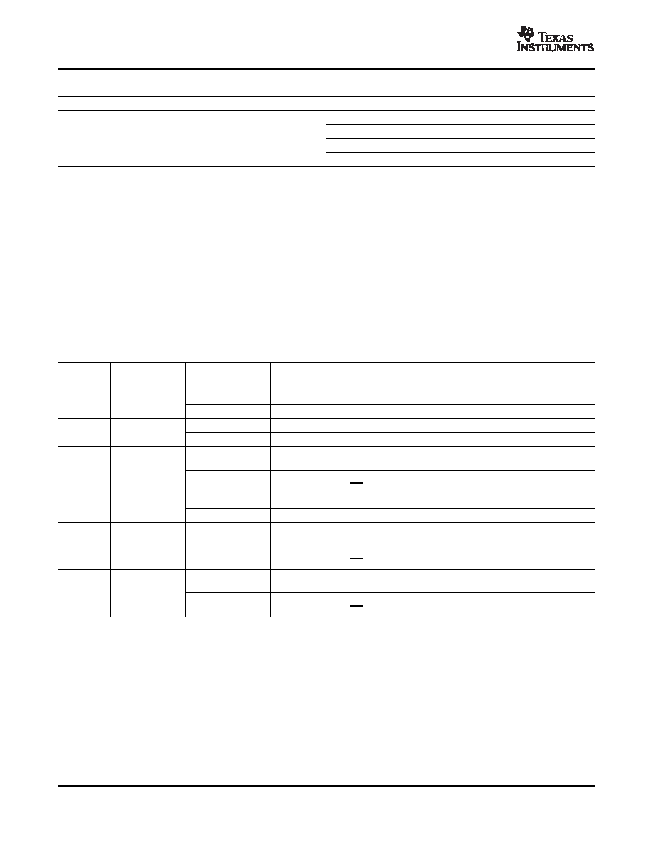
Table 3. TMDS442 Sink Port Register Bit Decoder (continued)
BIT
FUNCTION
BIT VALUES
RESULT
00
Source port 1 select
01
Source port 2 select
1, 0
SB SA
10
Source port 3 select
11
Source port 4 select
Bits 7 (MSB), 6 and 5 – Reserved bits without function.
Bit 4 – Controls the TMDS output differential voltage.
Bit 3 – Controls the status of DDC interface, SCL_SINK and
SDA_SINK.
Bit 2 – Controls the status of TMDS interface, Y/Z.
Bits 1, and 0 (LSB) – Selects the source input of the TMDS442.
The 5-V plug in status can be read through each bit of the sub-address (source plug-in status) status register.
Each bit of the third sub-address, source plug-in status registers, allows the user to read the cable plug-in status
based on the appearance of a valid +5-V power signal from each source input port. The bit description is
decoded in Table 4.
Table 4. TMDS442 Source Plug-In Status Register Bit Decoder
BIT
FUNCTION
BIT VALUES
RESULT
7, 6
Reserved
0 0
Default value
0
Sink port1 is the main display when the same source is selected by both sinks
5
SP
1
Sink port2 is the main display when the same source is selected by both sinks
0
TMDS output status is not controlled by the corresponding +5-V power signal
4
5V_EN
1
TMDS output status is controlled by the corresponding +5-V power signal
0
Source side I2C buffer is disabled (Hi-Z) When source port 4 is selected by sink,
TMDS is Hi-Z
3
5V_PWR4
1
Source side I2C buffer is enabled When source port 4 is selected by sink, TMDS is
under the control of OE
0
Source side I2C buffer is disabled (Hi-Z)
2
5V_PWR3
1
When source port 3 is selected by sink, TMDS is Hi-Z
0
Source side I2C buffer is disabled (Hi-Z) When source port 2 is selected by sink,
TMDS is Hi-Z
1
5V_PWR2
1
Source side I2C buffer is enabled When source port 2 is selected by sink, TMDS is
under the control of OE
0
Source side I2C buffer is disabled (Hi-Z) When source port 1 is selected by sink,
TMDS is Hi-Z
0
5V_PWR1
1
Source side I2C buffer is enabled When source port 1 is selected by sink, TMDS is
under the control of OE
The proper way to write to the TMDS442 is illustrated as follows:
An I2C master initiates a write operation to the TMDS442 by generating a start condition (S) followed by the
TMDS442 I2C address (as shown below), in MSB first bit order, followed by a 0 to indicate a write cycle. After
receiving an acknowledge from the TMDS442, the master presents the sub-address (sink port) it wants to write
consisting of one byte of data, MSB first. The TMDS442 acknowledges the byte after completion of the transfer.
Finally the master presents the data it wants to write to the register (sink port) and the TMDS442 acknowledges
the byte. The I2C master then terminates the write operation by generating a stop condition (P). Note that the
TMDS442 does not support multi-byte transfers. To write to both sink ports – or registers - this procedure must
be repeated for each register one series at a time (i.e. repeat steps 1 through 8 for each sink port).
28
Copyright 2006–2007, Texas Instruments Incorporated
Product Folder Link(s): TMDS442
相關(guān)PDF資料 |
PDF描述 |
|---|---|
| TMDS461PZIT | SPECIALTY CONSUMER CIRCUIT, PQFP100 |
| TMDS461PZT | SPECIALTY CONSUMER CIRCUIT, PQFP100 |
| TMDS461PZTR | SPECIALTY CONSUMER CIRCUIT, PQFP100 |
| TMP431BDGKT | SPECIALTY ANALOG CIRCUIT, PDSO8 |
| TMP435ADGST | SPECIALTY ANALOG CIRCUIT, PDSO10 |
相關(guān)代理商/技術(shù)參數(shù) |
參數(shù)描述 |
|---|---|
| TMDS461 | 制造商:TI 制造商全稱:Texas Instruments 功能描述:1080p a?? Deep Color 4-to-1 HDMI/DVI Switch with Adaptive Equalization |
| TMDS461PZT | 功能描述:視頻開關(guān) IC 4 to 1 HDMI Switch RoHS:否 制造商:Texas Instruments 開關(guān)數(shù)量:4 開啟電阻(最大值):12 Ohms 傳播延遲時(shí)間: 開啟時(shí)間(最大值): 關(guān)閉時(shí)間(最大值): 最大工作溫度:+ 85 C 最小工作溫度:- 40 C 封裝 / 箱體:WQFN-42 封裝:Reel |
| TMDS461PZTR | 功能描述:視頻開關(guān) IC 4 to 1 HDMI Switch RoHS:否 制造商:Texas Instruments 開關(guān)數(shù)量:4 開啟電阻(最大值):12 Ohms 傳播延遲時(shí)間: 開啟時(shí)間(最大值): 關(guān)閉時(shí)間(最大值): 最大工作溫度:+ 85 C 最小工作溫度:- 40 C 封裝 / 箱體:WQFN-42 封裝:Reel |
| TMDS570LS12HDK | 功能描述:TMS570LS Hercules? MCU 32-Bit ARM? Cortex?-R4F Embedded Evaluation Board 制造商:texas instruments 系列:Hercules? 零件狀態(tài):有效 板類型:評(píng)估平臺(tái) 類型:MCU 32-位 核心處理器:ARM? Cortex?-R4F 操作系統(tǒng):- 平臺(tái):- 配套使用產(chǎn)品/相關(guān)產(chǎn)品:TMS570LS 安裝類型:固定 內(nèi)容:板,電纜,配件 標(biāo)準(zhǔn)包裝:1 |
| TMDS570LS31HDK | 制造商:Texas Instruments 功能描述:HERCULES DEVELOPMENT KIT |
發(fā)布緊急采購(gòu),3分鐘左右您將得到回復(fù)。