- 您現在的位置:買賣IC網 > PDF目錄98282 > TPS51317RGBR (TEXAS INSTRUMENTS INC) SWITCHING REGULATOR, 1500 kHz SWITCHING FREQ-MAX, PQCC20 PDF資料下載
參數資料
| 型號: | TPS51317RGBR |
| 廠商: | TEXAS INSTRUMENTS INC |
| 元件分類: | 穩壓器 |
| 英文描述: | SWITCHING REGULATOR, 1500 kHz SWITCHING FREQ-MAX, PQCC20 |
| 封裝: | 4 X 3.50 MM, GREEN, PLASTIC, QFN-20 |
| 文件頁數: | 23/28頁 |
| 文件大小: | 1000K |
| 代理商: | TPS51317RGBR |
第1頁第2頁第3頁第4頁第5頁第6頁第7頁第8頁第9頁第10頁第11頁第12頁第13頁第14頁第15頁第16頁第17頁第18頁第19頁第20頁第21頁第22頁當前第23頁第24頁第25頁第26頁第27頁第28頁
SLUSAH9
– MARCH 2011
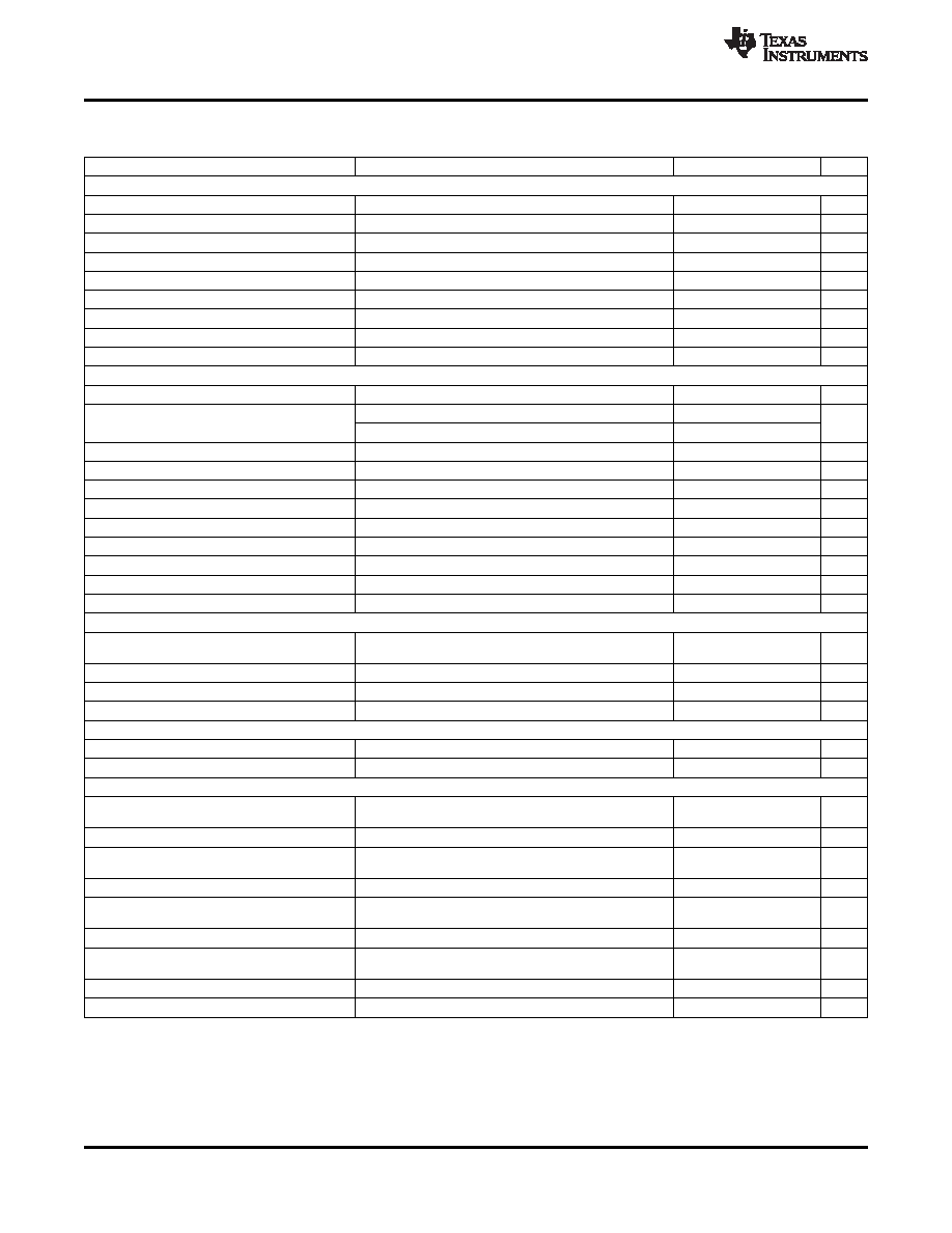
ELECTRICAL CHARACTERISTICS
over recommended free-air temperature range, VV5IN = 5.0 V, PGND = GND (unless otherwise noted)
PARAMETER
CONDITIONS
MIN
TYP
MAX
UNIT
SUPPLY: VOLTAGE, CURRENTS AND 5 V UVLO
IVINSD
VIN shutdown current
EN =
'LO'
0.02
5
A
V5VIN
5VIN supply voltage
V5IN voltage range
4.5
5.0
6.5
V
I5VIN
5VIN supply current
EN =
’HI’, V5IN supply current
1.1
2
mA
I5VINSD
5VIN shutdown current
EN =
‘LO’, V5IN shutdown current
0.2
7.0
A
VV5UVLO
V5IN UVLO
Ramp up; EN =
'HI'
4.20
4.37
4.50
V
VV5UVHYS
V5IN UVLO hysteresis
Falling hysteresis
440
mV
VVREFUVLO
REF UVLO(1)
Rising edge of VREF, EN =
'HI'
1.8
V
VVREFUVHYS
REF UVLO hysteresis(1)
100
mV
VPOR5VFILT
Reset
OVP latch is reset by V5IN falling below the reset threshold
1.5
2.3
3.1
V
VOLTAGE FEEDBACK LOOP: VREF, VOUT, AND VOLTAGE GM AMPLIFIER
VOUTTOL
VOUT accuracy
VREFIN = 1 V, No droop
–1%
0%
1%
IVREF = 0 A
1.98
2.00
2.02
VVREF
VREF
V
IVREF = 50 A
1.975
2.000
2.025
IREFSNK
VREF sink current
VVREF = 2.05 V
2.5
mA
GM
Transconductance
1.00
mS
VCM
Common mode input voltage range(1)
0
2
V
VDM
Differential mode input voltage
0
80
mV
ICOMPSNK
COMP pin maximum sinking current
VCOMP = 2 V, (VREFIN - VOUT) = 80 mV
80
A
ICOMPSRC
COMP pin maximum sourcing current
VCOMP = 2 V
-80
A
VOFFSET
Input offset voltage
TA = 25°C
0
mV
RDSCH
Output voltage discharge resistance
42
Ω
f–3dbVL
–3dB Frequency(1)
4.5
6.0
7.5
MHz
CURRENT SENSE: CURRENT SENSE AMPLIFIER, OVERCURRENT AND ZERO CROSSING
Gain from the current of the low-side FET to PWM comparator
ACSINT
Internal current sense gain
43
53
57
mV/A
when PWM =
"OFF"
IOCL
Positive overcurrent limit (valley)
7.6
A
IOCL(neg)
Negative overcurrent limit (valley)
–9.3
A
VZXOFF
Zero crossing comp internal offset
0
mV
DRIVERS: BOOT STRAP SWITCH
RDSONBST
Internal BST switch on-resistance
IBST = 10 mA, TA = 25°C
10
Ω
IBSTLK
Internal BST switch leakage current
VBST = 14 V, VSW = 7 V
1
A
PROTECTION: OVP, UVP, PGOOD, and THERMAL SHUTDOWN
PGOOD deassert to lower
VPGDLL
Measured at the VOUT pin wrt/ VREFIN
84%
(PGOOD
→ Low)
VPGHYSHL
PGOOD high hysteresis
8%
PGOOD de-assert to higher
VPGDLH
Measured at the VOUT pin wrt/ VREFIN
116%
(PGOOD
→ Low)
VPGHYSHH
PGOOD high hysteresis
-8%
Minimum VIN voltage for valid
Measured at the VIN pin with a 2-mA sink current on PGOOD
VINMINPG
0.9
1.3
1.5
V
PGOOD
pin
VOVP
OVP threshold
Measured at the VOUT pin wrt/ VREFIN
117%
120%
123%
Measured at the VOUT pin wrt/ VREFIN, device latches OFF,
VUVP
UVP threshold
65%
68%
71%
begins soft-stop
THSD
Thermal shutdown(1)
Latch off controller, attempt soft-stop.
145
°C
THSD(hys)
Thermal Shutdown hysteresis(1)
Controller re-starts after temperature has dropped
10
°C
(1)
Ensured by design, not production tested.
4
Copyright
2011, Texas Instruments Incorporated
Product Folder Link(s): TPS51317
相關PDF資料 |
PDF描述 |
|---|---|
| TPS51427ARHBR | DUAL SWITCHING CONTROLLER, PQCC32 |
| TPS51427ARHBT | DUAL SWITCHING CONTROLLER, PQCC32 |
| TPS51461RGET | SWITCHING REGULATOR, 1000 kHz SWITCHING FREQ-MAX, PQCC24 |
| TPS51511RHLT | SWITCHING CONTROLLER, 350 kHz SWITCHING FREQ-MAX, PQCC20 |
| TPS53114PW | SWITCHING CONTROLLER, 700 kHz SWITCHING FREQ-MAX, PDSO16 |
相關代理商/技術參數 |
參數描述 |
|---|---|
| TPS51317RGBT | 功能描述:直流/直流開關轉換器 3.3V/5Vin,6A,DCAP Mode Sync Converter RoHS:否 制造商:STMicroelectronics 最大輸入電壓:4.5 V 開關頻率:1.5 MHz 輸出電壓:4.6 V 輸出電流:250 mA 輸出端數量:2 最大工作溫度:+ 85 C 安裝風格:SMD/SMT |
| TPS51362RVER | 制造商:Texas Instruments 功能描述:22V INPUT, 10A INTEGRATED FET 制造商:Texas Instruments 功能描述:IC REG BUCK SYNC ADJ 10A 28VQFN |
| TPS51362RVET | 制造商:Texas Instruments 功能描述:22V INPUT, 10A INTEGRATED FET 制造商:Texas Instruments 功能描述:IC REG BUCK SYNC ADJ 10A 28VQFN |
| TPS51363 | 制造商:TI 制造商全稱:Texas Instruments 功能描述:22-V Input, 8-A or 10-A Converter With Integrated FET |
| TPS51363RVER | 制造商:Texas Instruments 功能描述:Conv DC-DC Single Step Down 3V to 22V 28-Pin VQFN EP T/R 制造商:Texas Instruments 功能描述:IC REG BCK SYNC ADJ 10/8A 28VQFN |
發布緊急采購,3分鐘左右您將得到回復。