- 您現在的位置:買賣IC網 > PDF目錄382706 > U6268B-FP Low power JFET dual operational amplifiers PDF資料下載
參數資料
| 型號: | U6268B-FP |
| 英文描述: | Low power JFET dual operational amplifiers |
| 文件頁數: | 4/13頁 |
| 文件大小: | 109K |
| 代理商: | U6268B-FP |
U6268B
Rev. A3, 11-Apr-01
4 (13)
Functional Description
V
S
The IC and the external units are powered via the V
S
Pin 4. This pin is connected to the battery via a reverse
battery protection diode. An electrolythic capacitor of
22 F smoothes the voltage and absorbes positive and
negative transients.
OUT1, OUT2
OUTx provides a smoothed, very slowly changing supply
voltage for the external units and monitors the output cur-
rent. During normal operating conditions, the OUTx
voltage is typ. 3 V below V
S
, and changes very slowly
with a varying battery voltage in order to suppress distur-
bances in the data transmission. At low V
S
(5.7 to 8.5 V),
the OUTx voltage is typ. 0.5 V below V
S
. This voltage
difference is reduced in order to ensure sufficient supply
voltage for the external unit between OUTx and
RETURNx. The output current capability is 50 mA. The
internal pull-down current at OUTx is typically 3 mA.
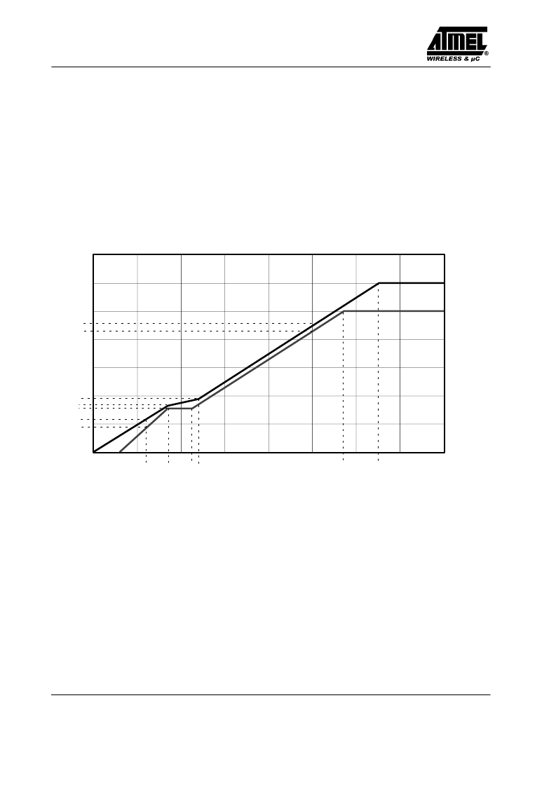
0
5
10
15
20
25
30
35
0
5
10
15
20
25
30
35
40
V
S
( V )
13322
o
22.4
21.4
9.4
8.2
7.7
5.4
4.9
5.7
8.5
11.3 12.0
28.6
32.6
Vout max
Vout min
V
Figure 4. Output voltage with tolerances vs. supply voltage
The data transmission from the external unit to the
interface IC is carried out on the same line by varying the
current level. The quiescent current consumption of the
external unit is about 5 to 15 mA. This current level is
interpreted as logic high level at CLL-pin. The external
unit can switch on an additional current of 30 mA,
interpreted by the interface as logic low. The current
changes within approximately 1 s, sufficient for a
transmission rate of about 60 kBaud, requiring a
transmission bandwidth of about 500 kHz for the current-
monitoring subcircuit and the OCM output. For a good
current transmission behaviour, the dynamic resistance of
OUTx may not exceed 12 inside the bandwidth range
(total of 15
for OUTx and RETURN).
The OUTx- voltage can be switched off by
ENABLEx = LOW to reset the external unit and to
reduce power dissipation during fault conditions.
The OUT pins are overtemperature- and short-circuit
protected. A reverse polarity diode at Pin V
S
(Pin 4) en-
sures that no current is fed back to the V
Batt
-system in the
case of a short between OUTx and V
Batt
. A minimum ca-
pacity of 33 nF is required at the pins OUTx.
相關PDF資料 |
PDF描述 |
|---|---|
| U6268B | Side-Airbag Sensor Dual Interface |
| U62H256SA35 | x8 SRAM |
| U62H256SA55 | x8 SRAM |
| U62H256SK35 | Low power JFET dual operational amplifiers |
| U62H256SK55 | x8 SRAM |
相關代理商/技術參數 |
參數描述 |
|---|---|
| U6268B-MFPG3 | 功能描述:IC INTERFACE DUAL SENSOR 16-SOIC RoHS:是 類別:集成電路 (IC) >> 接口 - 傳感器和探測器接口 系列:* 其它有關文件:Automotive Product Guide 產品培訓模塊:Lead (SnPb) Finish for COTS Obsolescence Mitigation Program 標準包裝:74 系列:- 類型:觸控式傳感器 輸入類型:數字 輸出類型:數字 接口:JTAG,串行 電流 - 電源:100µA 安裝類型:表面貼裝 封裝/外殼:20-TSSOP(0.173",4.40mm 寬) 供應商設備封裝:20-TSSOP 包裝:管件 |
| U6268B-MFPG3Y | 功能描述:射頻無線雜項 Sat.Interface (Airbag) RoHS:否 制造商:Texas Instruments 工作頻率:112 kHz to 205 kHz 電源電壓-最大:3.6 V 電源電壓-最小:3 V 電源電流:8 mA 最大功率耗散: 工作溫度范圍:- 40 C to + 110 C 封裝 / 箱體:VQFN-48 封裝:Reel |
| U629029B | 制造商: 功能描述: 制造商:undefined 功能描述: |
| U62H256A | 制造商:ZMD 制造商全稱:Zentrum Mikroelektronik Dresden AG 功能描述:AUTOMOTIVE FAST 32K X 8 SRAM |
| U62H256AS2A35 | 制造商:ZMD 制造商全稱:Zentrum Mikroelektronik Dresden AG 功能描述:AUTOMOTIVE FAST 32K X 8 SRAM |
發布緊急采購,3分鐘左右您將得到回復。