- 您現在的位置:買賣IC網 > PDF目錄373911 > AD7641 (Analog Devices, Inc.) 18-Bit, 2 MSPS SAR ADC PDF資料下載
參數資料
| 型號: | AD7641 |
| 廠商: | Analog Devices, Inc. |
| 英文描述: | 18-Bit, 2 MSPS SAR ADC |
| 中文描述: | 18位,2 MSPS的SAR型ADC |
| 文件頁數: | 14/24頁 |
| 文件大小: | 324K |
| 代理商: | AD7641 |
AD7641
Preliminary Technical Data
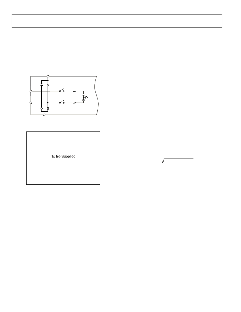
TYPICAL CONNECTION DIAGRAM
Figure 7 shows a typical connection diagram for the AD7641.
Different circuitry shown on this diagram are optional and are
discussed below.
Rev. Pr E | Page 14 of 24
ANALOG INPUTS
Figure 8 shows a simplified analog input section of the AD7641.
IN+
IN-
R+= 87
Cs
AGND
AVDD
R- = 87
Cs
Figure 8. AD7641 simplified Analog input
Figure 9. Analog Input CMRR vs. Frequency
During the acquisition phase, for AC signals, the AD7641
behaves like a one pole RC filter consisted of the equivalent
resistance R+ , R- and C
S
. The resistors R
+
and R
-
are typically
TBD and are lumped component made up of some serial
resistor and the on resistance of the switches. The capacitor C
S
is
typically TBD pF and is mainly the ADC sampling capacitor.
This one pole filter with a typical -3dB cutoff frequency of 50
MHz reduces undesirable aliasing effect and limits the noise
coming from the inputs.
Because the input impedance of the AD7641 is very high, the
AD7641 can be driven directly by a low impedance source
without gain error. This allows, as shown in Figure 7, an external
one-pole RC filter between the output of the amplifier and the
ADC analog inputs to even further improve the noise filtering
done by the AD7641 analog input circuit. However, the source
impedance has to be kept low because it affects the ac
performances, especially the total harmonic distortion. The
maximum source impedance depends on the amount of total
harmonic distortion (THD) that can be tolerated. The THD
degrades as a function of the source impedance and the
maximum input frequency.
DRIVER AMPLIFIER CHOICE
Although the AD7641 is easy to drive, the driver amplifier
needs to meet at least the following requirements:
The driver amplifier and the AD7641 analog input circuit
have to be able together to settle for a full-scale step the
capacitor array at a 18-bit level (0.0004%). In the amplifier’s
datasheet, the settling at 0.1% or 0.01% is more commonly
specified. It could significantly differ from the settling time
at 18 bit level and, therefore, it should be verified prior to
the driver selection. The tiny op-amp AD8021 which
combines ultra low noise and a high gain bandwidth meets
this settling time requirement.
The noise generated by the driver amplifier needs to be
kept as low as possible in order to preserve the SNR and
transition noise performance of the AD7641. The noise
coming from the driver is filtered by the AD7641 analog
input circuit one-pole low-pass filter made by R
+
, R
-
and C
S
.
The SNR degradation due to the amplifier is :
(
)
+
=
2
3
3136
56
f
20
N
dB
LOSS
Ne
LOG
SNR
π
where :
f
-3dB
is the -3dB input bandwidth in MHz of the AD7641 (50
MHz) or the cutoff frequency of the input filter if any used
N is the noise factor of the amplifiers ( 1 if in buffer
configuration)
e
N
is the equivalent input noise voltage of each op-amp in
nV/(Hz)
1/2
For instance, a driver with an equivalent input noise of
2nV/√Hz like the AD8021 and configured as a buffer, thus with
a noise gain of +1, the SNR degrades by only 0.17 dB with the
filter in Figure 7, and 0.8 dB without.
The driver needs to have a THD performance suitable to
that of the AD7641.
The AD8021 meets these requirements and is usually
appropriate for almost all applications. The AD8021 needs an
external compensation capacitor of 10 pF. This capacitor should
have good linearity as an NPO ceramic or mica type.
The AD8022 could also be used where dual version is needed
and gain of 1 is used.
The AD8027 is another option where lower supply and
dissipation are desired.
相關PDF資料 |
PDF描述 |
|---|---|
| AD7641ACP | 18-Bit, 2 MSPS SAR ADC |
| AD7641ACPRL | ECONOLINE: REC2.2-S_DRW(Z)/H* - 2.2W DIP Package- 1kVDC Isolation- Regulated Output- 4.5-9V, 9-18V, 18-36V, 36-72V Wide Input Range 2 : 1- UL94V-0 Package Material- Continuous Short Circiut Protection- Cost Effective- 100% Burned In- Efficiency to 84% |
| AD7641AST | 18-Bit, 2 MSPS SAR ADC |
| AD7641ASTRL | 18-Bit, 2 MSPS SAR ADC |
| AD7650 | 16-Bit 1 MSPS SAR Unipolar ADC with Ref |
相關代理商/技術參數 |
參數描述 |
|---|---|
| AD7641ACP | 制造商:Analog Devices 功能描述:ADC SGL SAR 2MSPS 18BIT PARALLEL/SERL 48LFCSP - Trays |
| AD7641ACPRL | 制造商:Analog Devices 功能描述:ADC SGL SAR 2MSPS 18BIT PARALLEL/SERL 48LFCSP - Tape and Reel |
| AD7641AST | 制造商:Analog Devices 功能描述:ADC SGL SAR 2MSPS 18BIT PARALLEL/SERL 48LQFP - Bulk |
| AD7641ASTRL | 制造商:Analog Devices 功能描述:ADC SGL SAR 2MSPS 18BIT PARALLEL/SERL 48LQFP - Tape and Reel |
| AD7641BCPZ | 功能描述:IC ADC 18BIT 2MSPS SAR 48-LFCSP RoHS:是 類別:集成電路 (IC) >> 數據采集 - 模數轉換器 系列:- 其它有關文件:TSA1204 View All Specifications 標準包裝:1 系列:- 位數:12 采樣率(每秒):20M 數據接口:并聯 轉換器數目:2 功率耗散(最大):155mW 電壓電源:模擬和數字 工作溫度:-40°C ~ 85°C 安裝類型:表面貼裝 封裝/外殼:48-TQFP 供應商設備封裝:48-TQFP(7x7) 包裝:Digi-Reel® 輸入數目和類型:4 個單端,單極;2 個差分,單極 產品目錄頁面:1156 (CN2011-ZH PDF) 其它名稱:497-5435-6 |
發布緊急采購,3分鐘左右您將得到回復。