- 您現在的位置:買賣IC網 > PDF目錄373911 > AD7641 (Analog Devices, Inc.) 18-Bit, 2 MSPS SAR ADC PDF資料下載
參數資料
| 型號: | AD7641 |
| 廠商: | Analog Devices, Inc. |
| 英文描述: | 18-Bit, 2 MSPS SAR ADC |
| 中文描述: | 18位,2 MSPS的SAR型ADC |
| 文件頁數: | 15/24頁 |
| 文件大小: | 324K |
| 代理商: | AD7641 |
Preliminary Technical Data
AD7641
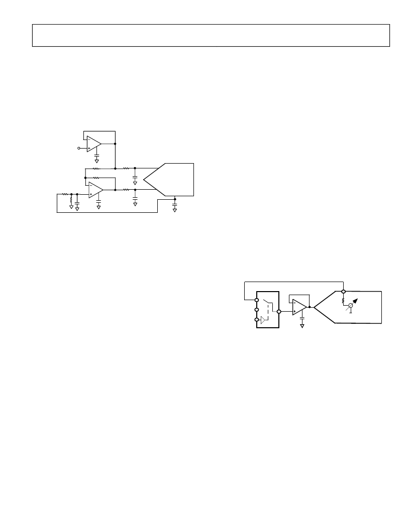
SINGLE TO DIFFERENTIAL DRIVER
For applications using unipolar analog signals, a single ended to
differential driver will allow for a differential input into the part.
The schematic is shown in Figure 10. This configuration, when
provided an input signal of 0 to V
REF
, will produce a differential
±V
REF
with midscale at V
REF
/2.
Rev. Pr E | Page 15 of 24
If the application can tolerate more noise, the AD8138 – a
differential driver, can be used.
10pF
U2
590
AD8021
ANALOG INPUT
(UNIPOLAR 0 to 2.5V)
10pF
U1
590
AD8021
IN+
AD7641
IN-
10k
10k
REF
10 F
15
15
100nF
1nF
1nF
Figure 10. Single Ended to Differential Driver Circuit
(Internal Reference Buffer Used)
VOLTAGE REFERENCE
The AD7641 allows the choice of either a very low temperature
drift internal voltage reference or an external reference.
Unlike many ADC with internal reference, the internal
reference of the AD7641 provides excellent performances and
can be used in almost all applications. It is temperature
compensated to 1.2V ± TBD mV with a typical drift of TBD
ppm/°C, a typical long-term stability of TBD ppm and a typical
hysterisis of TBD ppm.
However, the advantages to use the external reference voltage
directly are :
The power saving of about 8mW typical when the internal
reference and its buffer are powered down ( PDREF and
PDBUF High )
The SNR and dynamic range improvement of about 1.7 dB
resulting of the use of a reference voltage very close to the
supply (2.5V) instead of a typical 2.048V reference when
the internal buffer is used.
To use the internal reference along with the internal buffer,
PDREF and PDBUF should both be LOW. This will produce a
voltage on REFBUFIN of 1.2 V and the buffer will amplify it
resulting in a 2.048 V reference on REF pin.
It is useful to decouple the REFBUFIN pin with a 100 nF
ceramic capacitor. The output impedance of the REFBUFIN pin
is 16 k. Thus, the 100 nF capacitor provides an RC filter for
noise reduction.
To use an external reference along with the internal buffer,
PDREF should be HIGH and PDBUF should be low. This
powers down the internal reference and allows for the 1.2 V
reference to be applied to REFBUFIN.
To use an external reference directly on REF pin, PDREF and
PDBUF should both be HIGH.
It should be noted that the internal reference and internal buffer
are independent of the power down (PD) pin of the part.
Furthermore, powering up the internal reference and internal
buffer requires time due to the charge of the REF decoupling.
In both cases, the voltage reference input REF has a dynamic
input impedance and requires, therefore, an efficient decoupling
between REF and REFGND inputs. When the internal reference
buffer is used, this decoupling consists of a 10 μF ceramic
capacitor ( e.g. : Panasonic ECJ-3xB0J106 1206 size ).
When external reference is used, the decoupling consists of a
low ESR 47 μF tantalum capacitor connected to the REF and
REFGND inputs with minimum parasitic inductance.
TEMPERATURE SENSOR
The TEMP pin, which measures the temperature of the
AD7641, can be used as shown in Figure 11. The output of the
TEMP pin is applied to one of the inputs of the analog switch
(e.g. : ADG779) and the ADC itself is used to measure its own
temperature. This configuration could be very useful to improve
the calibration accuracy over the temperature range.
CC
AD8021
IN
AD7641
IN
temperature
sensor
ADG779
TEMP
Analog Input
(unipolar)
Figure 11. Use of the Temperature Sensor
相關PDF資料 |
PDF描述 |
|---|---|
| AD7641ACP | 18-Bit, 2 MSPS SAR ADC |
| AD7641ACPRL | ECONOLINE: REC2.2-S_DRW(Z)/H* - 2.2W DIP Package- 1kVDC Isolation- Regulated Output- 4.5-9V, 9-18V, 18-36V, 36-72V Wide Input Range 2 : 1- UL94V-0 Package Material- Continuous Short Circiut Protection- Cost Effective- 100% Burned In- Efficiency to 84% |
| AD7641AST | 18-Bit, 2 MSPS SAR ADC |
| AD7641ASTRL | 18-Bit, 2 MSPS SAR ADC |
| AD7650 | 16-Bit 1 MSPS SAR Unipolar ADC with Ref |
相關代理商/技術參數 |
參數描述 |
|---|---|
| AD7641ACP | 制造商:Analog Devices 功能描述:ADC SGL SAR 2MSPS 18BIT PARALLEL/SERL 48LFCSP - Trays |
| AD7641ACPRL | 制造商:Analog Devices 功能描述:ADC SGL SAR 2MSPS 18BIT PARALLEL/SERL 48LFCSP - Tape and Reel |
| AD7641AST | 制造商:Analog Devices 功能描述:ADC SGL SAR 2MSPS 18BIT PARALLEL/SERL 48LQFP - Bulk |
| AD7641ASTRL | 制造商:Analog Devices 功能描述:ADC SGL SAR 2MSPS 18BIT PARALLEL/SERL 48LQFP - Tape and Reel |
| AD7641BCPZ | 功能描述:IC ADC 18BIT 2MSPS SAR 48-LFCSP RoHS:是 類別:集成電路 (IC) >> 數據采集 - 模數轉換器 系列:- 其它有關文件:TSA1204 View All Specifications 標準包裝:1 系列:- 位數:12 采樣率(每秒):20M 數據接口:并聯 轉換器數目:2 功率耗散(最大):155mW 電壓電源:模擬和數字 工作溫度:-40°C ~ 85°C 安裝類型:表面貼裝 封裝/外殼:48-TQFP 供應商設備封裝:48-TQFP(7x7) 包裝:Digi-Reel® 輸入數目和類型:4 個單端,單極;2 個差分,單極 產品目錄頁面:1156 (CN2011-ZH PDF) 其它名稱:497-5435-6 |
發布緊急采購,3分鐘左右您將得到回復。