- 您現在的位置:買賣IC網 > PDF目錄373913 > AD7679CB1 (Analog Devices, Inc.) 18-Bit, 2.5 LSB INL, 570 kSPS SAR ADC PDF資料下載
參數資料
| 型號: | AD7679CB1 |
| 廠商: | Analog Devices, Inc. |
| 英文描述: | 18-Bit, 2.5 LSB INL, 570 kSPS SAR ADC |
| 中文描述: | 18位,2.5 LSB INL和570 kSPS的SAR型ADC |
| 文件頁數: | 22/28頁 |
| 文件大小: | 506K |
| 代理商: | AD7679CB1 |
第1頁第2頁第3頁第4頁第5頁第6頁第7頁第8頁第9頁第10頁第11頁第12頁第13頁第14頁第15頁第16頁第17頁第18頁第19頁第20頁第21頁當前第22頁第23頁第24頁第25頁第26頁第27頁第28頁
AD7679
RDC/SDIN = 1
INVSCLK = INVSYNC = 0
D17
D16
D2
D1
D0
X
1
2
3
16
17
18
BUSY
SYNC
SCLK
SDOUT
CS, RD
CNVST
t
3
t
1
t
17
t
14
t
15
t
19
t
20
t
21
t
16
t
22
t
23
t
24
t
27
t
26
t
25
t
18
EXT/INT = 0
03085-0-041
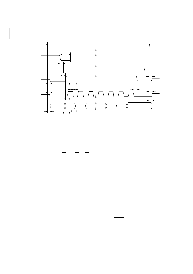
Figure 39. Master Serial Data Timing for Reading (Read Previous Conversion during Convert)
SLAVE SERIAL INTERFACE
External Clock
The AD7679 is configured to accept an externally supplied
serial data clock on the SCLK pin when the EXT/INT pin is
held high. In this mode, several methods can be used to read the
data. The external serial clock is gated by CS. When CS and RD
are both low, the data can be read after each conversion or
during the following conversion. The external clock can be
either a continuous or a discontinuous clock. A discontinuous
clock can be either normally high or normally low when
inactive. Figure 40 and Figure 41 show the detailed timing
diagrams of these methods.
While the AD7679 is performing a bit decision, it is important
that voltage transients not occur on digital input/output pins or
degradation of the conversion result could occur. This is
particularly important during the second half of the conversion
phase because the AD7679 provides error correction circuitry
that can correct for an improper bit decision made during the
first half of the conversion phase. For this reason, it is
recommended that when an external clock is being provided, it
is a discontinuous clock that toggles only when BUSY is low or,
more importantly, that it does not transition during the latter
half of BUSY high.
External Discontinuous Clock Data Read after
Conversion
This mode is the most recommended of the serial slave modes.
Figure 40 shows the detailed timing diagrams of this method.
After a conversion is complete, indicated by BUSY returning
low, the result of this conversion can be read while both CS and
RD are low. Data is shifted out MSB first with 18 clock pulses,
and is valid on the rising and falling edge of the clock.
Among the advantages of this method, the conversion
performance is not degraded because there are no voltage
transients on the digital interface during the conversion process.
Also, data can be read at speeds up to 40 MHz, accommodating
both slow digital host interface and the fastest serial reading.
Finally, in this mode only, the AD7679 provides a daisy-chain
feature using the RDC/SDIN input pin to cascade multiple
converters together. This feature is useful for reducing
component count and wiring connections when desired (for
instance, in isolated multiconverter applications).
An example of the concatenation of two devices is shown in
Figure 42. Simultaneous sampling is possible by using a
common CNVST signal. It should be noted that the RDC/SDIN
input is latched on the edge of SCLK opposite the one used to
shift out data on SDOUT. Thus, the MSB of the upstream
converter follows the LSB of the downstream converter on the
next SCLK cycle.
Rev. 0 | Page 22 of 28
相關PDF資料 |
PDF描述 |
|---|---|
| AD7694 | 16-Bit, 250 kSPS PulSAR ADC in MSOP |
| AD7694ARM | 16-Bit, 250 kSPS PulSAR ADC in MSOP |
| AD7694ARMRL7 | 16-Bit, 250 kSPS PulSAR ADC in MSOP |
| AD7694BRM | 16-Bit, 250 kSPS PulSAR ADC in MSOP |
| AD7694BRMRL7 | 16-Bit, 250 kSPS PulSAR ADC in MSOP |
相關代理商/技術參數 |
參數描述 |
|---|---|
| AD767A | 制造商:AD 制造商全稱:Analog Devices 功能描述:Microprocessor-Compatible 12-Bit D/A Converter |
| AD767ACHIPS | 制造商:AD 制造商全稱:Analog Devices 功能描述:Microprocessor-Compatible 12-Bit D/A Converter |
| AD767AD | 功能描述:IC DAC 12BIT W/AMP 24-CDIP RoHS:否 類別:集成電路 (IC) >> 數據采集 - 數模轉換器 系列:- 產品培訓模塊:Data Converter Fundamentals DAC Architectures 標準包裝:750 系列:- 設置時間:7µs 位數:16 數據接口:并聯 轉換器數目:1 電壓電源:雙 ± 功率耗散(最大):100mW 工作溫度:0°C ~ 70°C 安裝類型:表面貼裝 封裝/外殼:28-LCC(J 形引線) 供應商設備封裝:28-PLCC(11.51x11.51) 包裝:帶卷 (TR) 輸出數目和類型:1 電壓,單極;1 電壓,雙極 采樣率(每秒):143k |
| AD767BD | 功能描述:IC DAC 12BIT W/AMP 24-CDIP RoHS:否 類別:集成電路 (IC) >> 數據采集 - 數模轉換器 系列:- 產品培訓模塊:Lead (SnPb) Finish for COTS Obsolescence Mitigation Program 標準包裝:1,000 系列:- 設置時間:1µs 位數:8 數據接口:串行 轉換器數目:8 電壓電源:雙 ± 功率耗散(最大):941mW 工作溫度:0°C ~ 70°C 安裝類型:表面貼裝 封裝/外殼:24-SOIC(0.295",7.50mm 寬) 供應商設備封裝:24-SOIC W 包裝:帶卷 (TR) 輸出數目和類型:8 電壓,單極 采樣率(每秒):* |
| AD767JN | 功能描述:IC DAC 12BIT 24-DIP RoHS:否 類別:集成電路 (IC) >> 數據采集 - 數模轉換器 系列:- 產品培訓模塊:Data Converter Fundamentals DAC Architectures 標準包裝:750 系列:- 設置時間:7µs 位數:16 數據接口:并聯 轉換器數目:1 電壓電源:雙 ± 功率耗散(最大):100mW 工作溫度:0°C ~ 70°C 安裝類型:表面貼裝 封裝/外殼:28-LCC(J 形引線) 供應商設備封裝:28-PLCC(11.51x11.51) 包裝:帶卷 (TR) 輸出數目和類型:1 電壓,單極;1 電壓,雙極 采樣率(每秒):143k |
發布緊急采購,3分鐘左右您將得到回復。