- 您現(xiàn)在的位置:買(mǎi)賣(mài)IC網(wǎng) > PDF目錄373913 > AD7679CB1 (Analog Devices, Inc.) 18-Bit, 2.5 LSB INL, 570 kSPS SAR ADC PDF資料下載
參數(shù)資料
| 型號(hào): | AD7679CB1 |
| 廠商: | Analog Devices, Inc. |
| 英文描述: | 18-Bit, 2.5 LSB INL, 570 kSPS SAR ADC |
| 中文描述: | 18位,2.5 LSB INL和570 kSPS的SAR型ADC |
| 文件頁(yè)數(shù): | 24/28頁(yè) |
| 文件大小: | 506K |
| 代理商: | AD7679CB1 |
第1頁(yè)第2頁(yè)第3頁(yè)第4頁(yè)第5頁(yè)第6頁(yè)第7頁(yè)第8頁(yè)第9頁(yè)第10頁(yè)第11頁(yè)第12頁(yè)第13頁(yè)第14頁(yè)第15頁(yè)第16頁(yè)第17頁(yè)第18頁(yè)第19頁(yè)第20頁(yè)第21頁(yè)第22頁(yè)第23頁(yè)當(dāng)前第24頁(yè)第25頁(yè)第26頁(yè)第27頁(yè)第28頁(yè)
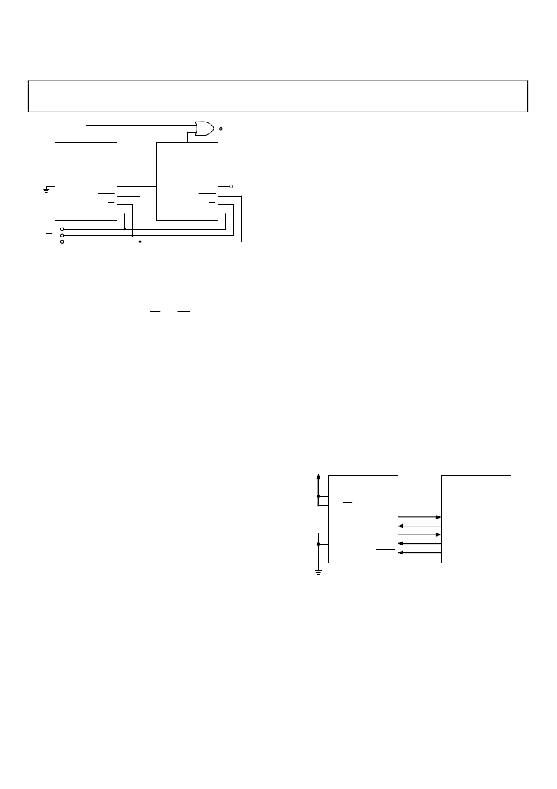
AD7679
BUSY
BUSY
AD7679
#2 (UPSTREAM)
AD7679
#1 (DOWNSTREAM)
RDC/SDIN
SDOUT
CNVST
CS
SCLK
RDC/SDIN
SDOUT
CNVST
CS
SCLK
DATA
OUT
SCLK IN
CS IN
CNVST IN
BUSY
OUT
03085-0-044
Figure 42. Two AD7679s in a Daisy-Chain Configuration
External Clock Data Read during Conversion
Figure 41 shows the detailed timing diagrams of this method.
During a conversion, while both CS and RD are low, the result
of the previous conversion can be read. The data is shifted out
MSB first with 18 clock pulses, and is valid on both the rising
and falling edge of the clock. The 18 bits have to be read before
the current conversion is complete. If that is not done,
RDERROR is pulsed high and can be used to interrupt the host
interface to prevent incomplete data reading. There is no daisy-
chain feature in this mode, and the RDC/SDIN input should
always be tied either high or low.
To reduce performance degradation due to digital activity, a fast
discontinuous clock is recommended to ensure that all bits are
read during the first half of the conversion phase. It is also
possible to begin to read the data after conversion and continue
to read the last bits even after a new conversion has been
initiated.
MICROPROCESSOR INTERFACING
The AD7679 is ideally suited for traditional dc measurement
applications supporting a microprocessor, and for ac signal
processing applications interfacing to a digital signal processor.
The AD7679 is designed to interface either with a parallel 8-bit
or 16-bit wide interface, or with a general-purpose serial port or
I/O ports on a microcontroller. A variety of external buffers can
be used with the AD7679 to prevent digital noise from coupling
into the ADC. The following section illustrates the use of the
AD7679 with an SPI equipped DSP, the ADSP-219x.
SPI Interface (ADSP-219x)
Figure 43 shows an interface diagram between the AD7679 and
the SPI equipped ADSP-219x. To accommodate the slower
speed of the DSP, the AD7679 acts as a slave device, and data
must be read after conversion. This mode also allows the daisy-
chain feature. The convert command could be initiated in
response to an internal timer interrupt. The 18-bit output data
are read with 3-byte SPI access. The reading process could be
initiated in response to the end-of-conversion signal (BUSY
going low) using an interrupt line of the DSP. The serial
interface (SPI) on the ADSP-219x is configured for master
mode (MSTR) = 1, Clock Polarity Bit (CPOL) = 0, Clock Phase
Bit (CPHA) = 1, and SPI interrupt enable (TIMOD) = 00, by
writing to the SPI Control register (SPICLTx). It should be
noted that to meet all timing requirements, the SPI clock should
be limited to 17 Mbits/s, which allow it to read an ADC result in
about 1.1 μs. When a higher sampling rate is desired, use of one
of the parallel interface modes is recommended.
AD7679*
ADSP-219x*
SER/PAR
PFx
MISOx
SCKx
PFx or TFSx
BUSY
SDOUT
SCLK
CNVST
EXT/INT
CS
RD
INVSCLK
DVDD
*ADDITIONAL PINS OMITTED FOR CLARITY
SPIxSEL (PFx)
03085-0-045
Figure 43. Interfacing the AD7679 to an SPI Interface
Rev. 0 | Page 24 of 28
相關(guān)PDF資料 |
PDF描述 |
|---|---|
| AD7694 | 16-Bit, 250 kSPS PulSAR ADC in MSOP |
| AD7694ARM | 16-Bit, 250 kSPS PulSAR ADC in MSOP |
| AD7694ARMRL7 | 16-Bit, 250 kSPS PulSAR ADC in MSOP |
| AD7694BRM | 16-Bit, 250 kSPS PulSAR ADC in MSOP |
| AD7694BRMRL7 | 16-Bit, 250 kSPS PulSAR ADC in MSOP |
相關(guān)代理商/技術(shù)參數(shù) |
參數(shù)描述 |
|---|---|
| AD767A | 制造商:AD 制造商全稱:Analog Devices 功能描述:Microprocessor-Compatible 12-Bit D/A Converter |
| AD767ACHIPS | 制造商:AD 制造商全稱:Analog Devices 功能描述:Microprocessor-Compatible 12-Bit D/A Converter |
| AD767AD | 功能描述:IC DAC 12BIT W/AMP 24-CDIP RoHS:否 類(lèi)別:集成電路 (IC) >> 數(shù)據(jù)采集 - 數(shù)模轉(zhuǎn)換器 系列:- 產(chǎn)品培訓(xùn)模塊:Data Converter Fundamentals DAC Architectures 標(biāo)準(zhǔn)包裝:750 系列:- 設(shè)置時(shí)間:7µs 位數(shù):16 數(shù)據(jù)接口:并聯(lián) 轉(zhuǎn)換器數(shù)目:1 電壓電源:雙 ± 功率耗散(最大):100mW 工作溫度:0°C ~ 70°C 安裝類(lèi)型:表面貼裝 封裝/外殼:28-LCC(J 形引線) 供應(yīng)商設(shè)備封裝:28-PLCC(11.51x11.51) 包裝:帶卷 (TR) 輸出數(shù)目和類(lèi)型:1 電壓,單極;1 電壓,雙極 采樣率(每秒):143k |
| AD767BD | 功能描述:IC DAC 12BIT W/AMP 24-CDIP RoHS:否 類(lèi)別:集成電路 (IC) >> 數(shù)據(jù)采集 - 數(shù)模轉(zhuǎn)換器 系列:- 產(chǎn)品培訓(xùn)模塊:Lead (SnPb) Finish for COTS Obsolescence Mitigation Program 標(biāo)準(zhǔn)包裝:1,000 系列:- 設(shè)置時(shí)間:1µs 位數(shù):8 數(shù)據(jù)接口:串行 轉(zhuǎn)換器數(shù)目:8 電壓電源:雙 ± 功率耗散(最大):941mW 工作溫度:0°C ~ 70°C 安裝類(lèi)型:表面貼裝 封裝/外殼:24-SOIC(0.295",7.50mm 寬) 供應(yīng)商設(shè)備封裝:24-SOIC W 包裝:帶卷 (TR) 輸出數(shù)目和類(lèi)型:8 電壓,單極 采樣率(每秒):* |
| AD767JN | 功能描述:IC DAC 12BIT 24-DIP RoHS:否 類(lèi)別:集成電路 (IC) >> 數(shù)據(jù)采集 - 數(shù)模轉(zhuǎn)換器 系列:- 產(chǎn)品培訓(xùn)模塊:Data Converter Fundamentals DAC Architectures 標(biāo)準(zhǔn)包裝:750 系列:- 設(shè)置時(shí)間:7µs 位數(shù):16 數(shù)據(jù)接口:并聯(lián) 轉(zhuǎn)換器數(shù)目:1 電壓電源:雙 ± 功率耗散(最大):100mW 工作溫度:0°C ~ 70°C 安裝類(lèi)型:表面貼裝 封裝/外殼:28-LCC(J 形引線) 供應(yīng)商設(shè)備封裝:28-PLCC(11.51x11.51) 包裝:帶卷 (TR) 輸出數(shù)目和類(lèi)型:1 電壓,單極;1 電壓,雙極 采樣率(每秒):143k |
發(fā)布緊急采購(gòu),3分鐘左右您將得到回復(fù)。