- 您現(xiàn)在的位置:買賣IC網(wǎng) > PDF目錄373915 > AD7721SQ (ANALOG DEVICES INC) CMOS 16-Bit, 468.75 kHz, Sigma-Delta ADC PDF資料下載
參數(shù)資料
| 型號(hào): | AD7721SQ |
| 廠商: | ANALOG DEVICES INC |
| 元件分類: | ADC |
| 英文描述: | CMOS 16-Bit, 468.75 kHz, Sigma-Delta ADC |
| 中文描述: | 1-CH 16-BIT DELTA-SIGMA ADC, SERIAL/PARALLEL ACCESS, CDIP28 |
| 封裝: | CERDIP-28 |
| 文件頁數(shù): | 5/16頁 |
| 文件大小: | 259K |
| 代理商: | AD7721SQ |
AD7721
REV. A
–5–
ABSOLUT E MAX IMUM RAT INGS
1
(T
A
= +25
°
C unless otherwise stated)
DV
DD
to DGND . . . . . . . . . . . . . . . . . . . . . . . –0.3 V to +7 V
AV
DD
to AGND . . . . . . . . . . . . . . . . . . . . . . . –0.3 V to +7 V
AV
DD
to DV
DD
. . . . . . . . . . . . . . . . . . . . . . –0.3 V to +0.3 V
AGND to DGND . . . . . . . . . . . . . . . . . . . . –0.3 V to +0.3 V
Digital Input Voltage to DGND . . . –0.3 V to DV
DD
+ 0.3 V
Analog Input Voltage to AGND . . . . –0.3 V to AV
DD
+ 0.3 V
Input Current to Any Pin Except Supplies
2
Operating T emperature Range
Industrial (A Version) . . . . . . . . . . . . . . . . . –40
°
C to +85
°
C
Extended (S Version) . . . . . . . . . . . . . . . . –55
°
C to +125
°
C
Storage T emperature Range . . . . . . . . . . . . –65
°
C to +150
°
C
Maximum Junction T emperature . . . . . . . . . . . . . . . +150
°
C
Plastic Package
θ
JA
T hermal Impedance . . . . . . . . . . . . . . . . . . . . . 74
°
C/W
. . . . . . .
±
10 mA
Lead T emperature, Soldering (10 sec) . . . . . . . . . . +260
°
C
Cerdip Package
θ
JA
T hermal Impedance . . . . . . . . . . . . . . . . . . . . . 51
°
C/W
Lead T emperature, Soldering (10 sec) . . . . . . . . . . +300
°
C
SOIC Package
θ
JA
T hermal Impedance . . . . . . . . . . . . . . . . . . . . . 72
°
C/W
Lead T emperature, Soldering
Vapor Phase (60 sec) . . . . . . . . . . . . . . . . . . . . . . +215
°
C
Infrared (15 sec) . . . . . . . . . . . . . . . . . . . . . . . . . +220
°
C
NOT ES
1
Stresses above those listed under Absolute Maximum Ratings may cause perma-
nent damage to the device. T his is a stress rating only; functional operation of the
device at these or any other conditions above those listed in the operational
sections of this specification is not implied. Exposure to absolute maximum
rating conditions for extended periods may affect device reliability.
2
T ransient currents of up to 100 mA will not cause SCR latchup.
C AUT ION
ESD (electrostatic discharge) sensitive device. Electrostatic charges as high as 4000 V readily
accumulate on the human body and test equipment and can discharge without detection.
Although this device features proprietary ESD protection circuitry, permanent damage may
occur on devices subjected to high energy electrostatic discharges. T herefore, proper ESD
precautions are recommended to avoid performance degradation or loss of functionality.
ORDE RING GUIDE
Model
T emperature Range
–40
°
C to +85
°
C
–40
°
C to +85
°
C
–55
°
C to +125
°
C
Package Option*
AD7721AN
AD7721AR
AD7721SQ
N-28
R-28
Q-28
*N = Plastic DIP; R = 0.3" Small Outline IC (SOIC); Q = Cerdip.
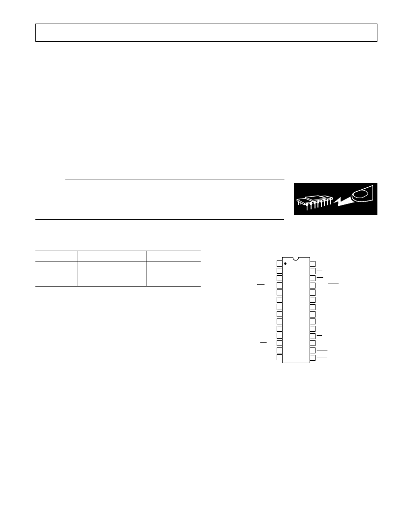
PIN CONFIGURAT ION
14
13
12
11
17
16
15
20
19
18
10
9
8
1
2
3
4
7
6
5
TOP VIEW
(Not to Scale)
28
27
26
25
24
23
22
21
AD7721
SCLK/DB7
DVAL/
SYNC
WR
RD
DB6
DB8
DB9
RFS
/DB10
SDATA/DB11
VIN1
VIN2
AGND
DGND
DSUBST
DGND
STBY/DB0
DV
DD
AV
DD
AGND
REFIN
CAL/DB1
UNI
/DB2
DB3
DB4
CS
CLK
SYNC
/DB5
DRDY
WARNNG
ESD SENSITIVE DEVICE
相關(guān)PDF資料 |
PDF描述 |
|---|---|
| AD7722 | 16-Bit, 195 kSPS CMOS, Sigma-Delta ADC |
| AD7722AS | 16-Bit, 195 kSPS CMOS, Sigma-Delta ADC |
| AD7723 | 16-Bit, 1.2 MSPS CMOS, Sigma-Delta ADC |
| AD7723BS | 16-Bit, 1.2 MSPS CMOS, Sigma-Delta ADC |
| AD7724AST | Dual CMOS Modulators |
相關(guān)代理商/技術(shù)參數(shù) |
參數(shù)描述 |
|---|---|
| AD7722 | 制造商:AD 制造商全稱:Analog Devices 功能描述:16-Bit, 195 kSPS CMOS, Sigma-Delta ADC |
| AD7722AS | 制造商:Rochester Electronics LLC 功能描述:16-BIT SIGMA-DELTA CONVERTER I.C. - Bulk 制造商:Analog Devices 功能描述:A/D Converter (A-D) IC |
| AD7722AS-ES | 制造商:Rochester Electronics LLC 功能描述:- Bulk |
| AD7722ASZ | 功能描述:IC ADC 16BIT 195KSPS 44-MQFP RoHS:是 類別:集成電路 (IC) >> 數(shù)據(jù)采集 - 模數(shù)轉(zhuǎn)換器 系列:- 標(biāo)準(zhǔn)包裝:1 系列:- 位數(shù):14 采樣率(每秒):83k 數(shù)據(jù)接口:串行,并聯(lián) 轉(zhuǎn)換器數(shù)目:1 功率耗散(最大):95mW 電壓電源:雙 ± 工作溫度:0°C ~ 70°C 安裝類型:通孔 封裝/外殼:28-DIP(0.600",15.24mm) 供應(yīng)商設(shè)備封裝:28-PDIP 包裝:管件 輸入數(shù)目和類型:1 個(gè)單端,雙極 |
| AD7722CSZ | 制造商:Analog Devices 功能描述: |
發(fā)布緊急采購,3分鐘左右您將得到回復(fù)。