- 您現在的位置:買賣IC網 > PDF目錄373915 > AD7722 (Analog Devices, Inc.) 16-Bit, 195 kSPS CMOS, Sigma-Delta ADC PDF資料下載
參數資料
| 型號: | AD7722 |
| 廠商: | Analog Devices, Inc. |
| 元件分類: | ADC |
| 英文描述: | 16-Bit, 195 kSPS CMOS, Sigma-Delta ADC |
| 中文描述: | 16位,195 kSPS的的CMOS,Σ-Δ模數轉換器 |
| 文件頁數: | 19/24頁 |
| 文件大小: | 526K |
| 代理商: | AD7722 |
AD7722
–19–
REV. 0
SERIAL INTERFACE
The AD7722’s serial data interface port allows easy interfacing
to industry standard digital signal processors. The AD7722
operates solely in the master mode providing three serial data
output pins for transfer of the conversion results. The serial data
clock output (SCO), serial data output (SDO) and frame sync
output (FSO) are all synchronous with CLKIN. SCO frequency
is always one-half the CLKIN frequency. FSO is continuously
output at the conversion rate of the ADC (FCLKIN/64). The
generalized timing diagrams in Figure 2 show how the AD7722
may be used to transmit its conversion results.
Serial data shifts out of the SDO pin synchronous with SCO.
The FSO is used to frame the output data transmission to an
external device. An output data transmission is 32 SCO cycles
in duration. The serial data shifts out of the SDO pin MSB first,
LSB last for a duration of 16 SCO cycles. For the next 16 SCO
cycles SDO outputs zeros.
Two control inputs, SFMT and CFMT, select the format for
the serial data transmission. FSO is either a pulse (approxi-
mately one SCO cycle in duration) or a square wave with a
period of 32 SCO cycles, depending on the state of the SFMT.
The logic level applied to SFMT also determines if the serial
data is valid on the rising or falling edge of the SCO. The clock
format pin, CFMT, simply switches the phase of SCO for the
selected FSO format.
With a logic low level on SFMT and CFMT set low (Figure 4),
FSO pulses high for one SCO cycle at the beginning of a data
transmission frame. When FSO goes low, the MSB is available
on the SDO pin after the rising edge of SCO and can be latched
on the SCO falling edge.
With a logic high level on SFMT and CFMT set low (Figure 4),
the data on the SDO pin is available after the falling edge of
SCO and can be latched on the SCO rising edge. FSO goes low
at the beginning of a data transmission frame when the MSB is
available and returns high after 16 SCO cycles.
The Frame Sync Input (FSI) can be used if the AD7722
conversion process must be synchronized to an external source.
FSI is an optional signal; if FSI is grounded or tied high frame,
syncs are internally generated. Frame sync allows the conver-
sion data presented to the serial interface to be a filtered and
decimated result derived from a known point in time. FSI can
be applied once after power-up, or it can be a periodic signal,
synchronous to CLKIN, occurring every 64 CLKIN cycles.
When FSI is applied for the first time, or if a low to high transition
is detected that is not synchronized to the output word rate, the
next 127 conversions should be considered invalid while the
digital filter accumulates new samples. Figure 4 shows how the
frame sync signal resets the serial output interface and how the
AD7722 will begin to output its serial data transmission frame.
A common frame sync signal can be applied to two or more
AD7722s to synchronize them to a common master clock.
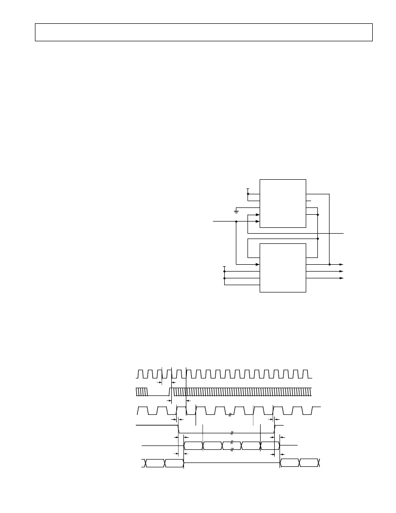
Two Channel Multiplexed Operation
Three additional serial interface control pins (DOE, TSI and
CFMT) are provided. The connection diagram in Figure 39
shows how they are used to allow the serial data outputs of two
AD7722s to easily share one serial data line. Since a serial data
transmission frame lasts 32 SCO cycles, two AD7722s can share
a single data line by alternating transmission of their 16-bit
output data onto one SDO pin.
CFMT
SDO
SFMT
SCO
TSI
FSO
FSI
DOE
CLKIN
AD7722
MASTER
FSI
DOE
CLKIN
SDO
CFMT
SCO
SFMT
FSO
TSI
AD7722
SLAVE
DV
DD
DV
DD
DGND
FROM
CONTROL
LOGIC
TO HOST
PROCESSOR
Figure 39. Connection for Two Channel Multiplexed
Operation
The Data Output Enable pin (DOE) controls SDO’s output
buffer. When the logic level on DOE matches the state of the
TSI pin, the SDO output buffer drives the serial dataline;
otherwise the output of the buffer goes high impedance. The
serial format pin (SFMT) is set high to chose the frame sync
output format. The clock format pin (CFMT) is set high so that
CLKIN
FSI
SCO
FSO (MASTER)
FSI (SLAVE)
DOE (MASTER & SLAVE)
t
1
t
14
t
12
t
11
t
16
t
15
t
15
t
16
SDO (MASTER)
SDO (SLAVE)
D15
D14
D1
D0
D15
D14
D1
D0
Figure 40. Timing for Two Channel Multiplexed Operation
相關PDF資料 |
PDF描述 |
|---|---|
| AD7722AS | 16-Bit, 195 kSPS CMOS, Sigma-Delta ADC |
| AD7723 | 16-Bit, 1.2 MSPS CMOS, Sigma-Delta ADC |
| AD7723BS | 16-Bit, 1.2 MSPS CMOS, Sigma-Delta ADC |
| AD7724AST | Dual CMOS Modulators |
| AD7724 | Dual CMOS Modulators |
相關代理商/技術參數 |
參數描述 |
|---|---|
| AD7722AS | 制造商:Rochester Electronics LLC 功能描述:16-BIT SIGMA-DELTA CONVERTER I.C. - Bulk 制造商:Analog Devices 功能描述:A/D Converter (A-D) IC |
| AD7722AS-ES | 制造商:Rochester Electronics LLC 功能描述:- Bulk |
| AD7722ASZ | 功能描述:IC ADC 16BIT 195KSPS 44-MQFP RoHS:是 類別:集成電路 (IC) >> 數據采集 - 模數轉換器 系列:- 標準包裝:1 系列:- 位數:14 采樣率(每秒):83k 數據接口:串行,并聯 轉換器數目:1 功率耗散(最大):95mW 電壓電源:雙 ± 工作溫度:0°C ~ 70°C 安裝類型:通孔 封裝/外殼:28-DIP(0.600",15.24mm) 供應商設備封裝:28-PDIP 包裝:管件 輸入數目和類型:1 個單端,雙極 |
| AD7722CSZ | 制造商:Analog Devices 功能描述: |
| AD7723 | 制造商:AD 制造商全稱:Analog Devices 功能描述:16-Bit, 1.2 MSPS CMOS, Sigma-Delta ADC |
發布緊急采購,3分鐘左右您將得到回復。