- 您現在的位置:買賣IC網 > PDF目錄373915 > AD7722 (Analog Devices, Inc.) 16-Bit, 195 kSPS CMOS, Sigma-Delta ADC PDF資料下載
參數資料
| 型號: | AD7722 |
| 廠商: | Analog Devices, Inc. |
| 元件分類: | ADC |
| 英文描述: | 16-Bit, 195 kSPS CMOS, Sigma-Delta ADC |
| 中文描述: | 16位,195 kSPS的的CMOS,Σ-Δ模數轉換器 |
| 文件頁數: | 3/24頁 |
| 文件大小: | 526K |
| 代理商: | AD7722 |
–3–
REV. 0
AD7722
A Version
Parameter
Test Conditions/Comments
Min
Typ
Max
Units
LOGIC INPUTS (Excluding CLKIN)
V
INH
, Input High Voltage
V
INL
, Input Low Voltage
2.0
V
V
0.8
CLOCK INPUT (CLKIN)
V
INH
, Input High Voltage
V
INL
, Input Low Voltage
4.0
V
V
0.4
ALL LOGIC INPUTS
I
IN
, Input Current
C
IN
, Input Capacitance
V
IN
= 0 V to DV
DD
±
10
10
μ
A
pF
LOGIC OUTPUTS
V
OH
, Output High Voltage
V
OL
, Output Low Voltage
|I
OUT
| = 200
μ
A
|I
OUT
| = 1.6 mA
4.0
V
V
0.4
POWER SUPPLIES
AV
DD
, AV
DD1
DV
DD
I
DD
Power Consumption
4.75
4.75
5.25
5.25
75
375
V
V
mA
mW
Total from AV
DD
and DV
DD
NOTES
1
Operating temperature range is as follows : A Version ; –40
°
C to +85
°
C.
2
Measurement Bandwidth = 0.5
×
F
S
; Input Level = –0.05 dB.
3
T
A
= +25
°
C to +85
°
C/T
A
= T
MIN
to T
MAX
.
4
Applies after calibration at temperature of interest.
5
Gain Error excludes reference error. The ADC gain is calibrated w.r.t. the voltage on the REF2 pin.
Specifications subject to change without notice.
ABSOLUTE MAXIMUM RATINGS*
(T
A
= +25
°
C unless otherwise noted)
DV
DD
to DGND . . . . . . . . . . . . . . . . . . . . . . . . –0.3 V to 7 V
AV
DD
, AV
DD1
to AGND . . . . . . . . . . . . . . . . . . –0.3 V to 7 V
AV
DD
, AV
DD1
to DVDD . . . . . . . . . . . . . . . . . . .–1 V to +1 V
AGND, AGND1 to DGND . . . . . . . . . . . . .–0.3 V to +0.3 V
Digital Inputs to DGND . . . . . . . . . . –0.3 V to DV
DD
+ 0.3 V
Digital Outputs to DGND . . . . . . . . . –0.3 V to DV
DD
+ 0.3 V
V
IN
(+), V
IN
(–) to AGND . . . . . . . . . . –0.3 V to AV
DD
+ 0.3 V
REF1 to AGND . . . . . . . . . . . . . . . . –0.3 V to AV
DD
+ 0.3 V
REF2 to AGND . . . . . . . . . . . . . . . . –0.3 V to AV
DD
+ 0.3 V
DGND, AGND1, AGND2 . . . . . . . . . . . . . . . . . . . . .
±
0.3 V
Operating Temperature Range . . . . . . . . . . . –40
°
C to +85
°
C
Storage Temperature Range . . . . . . . . . . . . –65
°
C to +150
°
C
Junction Temperature . . . . . . . . . . . . . . . . . . . . . . . . .+150
°
C
θ
JA
Thermal Impedance . . . . . . . . . . . . . . . . . . . . . . . 95
°
C/W
Lead Temperature, Soldering
Vapor Phase (60 sec) . . . . . . . . . . . . . . . . . . . . . . . .+215
°
C
Infrared (15 sec) . . . . . . . . . . . . . . . . . . . . . . . . . . . .+220
°
C
*Stresses above those listed under “Absolute Maximum Ratings” may cause
permanent damage to the device. This is a stress rating only and functional
operation of the device at these or any other conditions above those indicated in the
operational section of this specification is not implied. Exposure to absolute
maximum rating conditions for extended periods may affect device reliability.
WARNING!
ESD SENSITIVE DEVICE
CAUTION
ESD (electrostatic discharge) sensitive device. Electrostatic charges as high as 4000 V readily
accumulate on the human body and test equipment and can discharge without detection.
Although the AD7722 features proprietary ESD protection circuitry, permanent damage may
occur on devices subjected to high energy electrostatic discharges. Therefore, proper ESD
precautions are recommended to avoid performance degradation or loss of functionality.
ORDERING GUIDE
Model
Temperature
Package
Package
AD7722AS
–40
°
C to +85
°
C
44-Pin PQFP
S-44
I
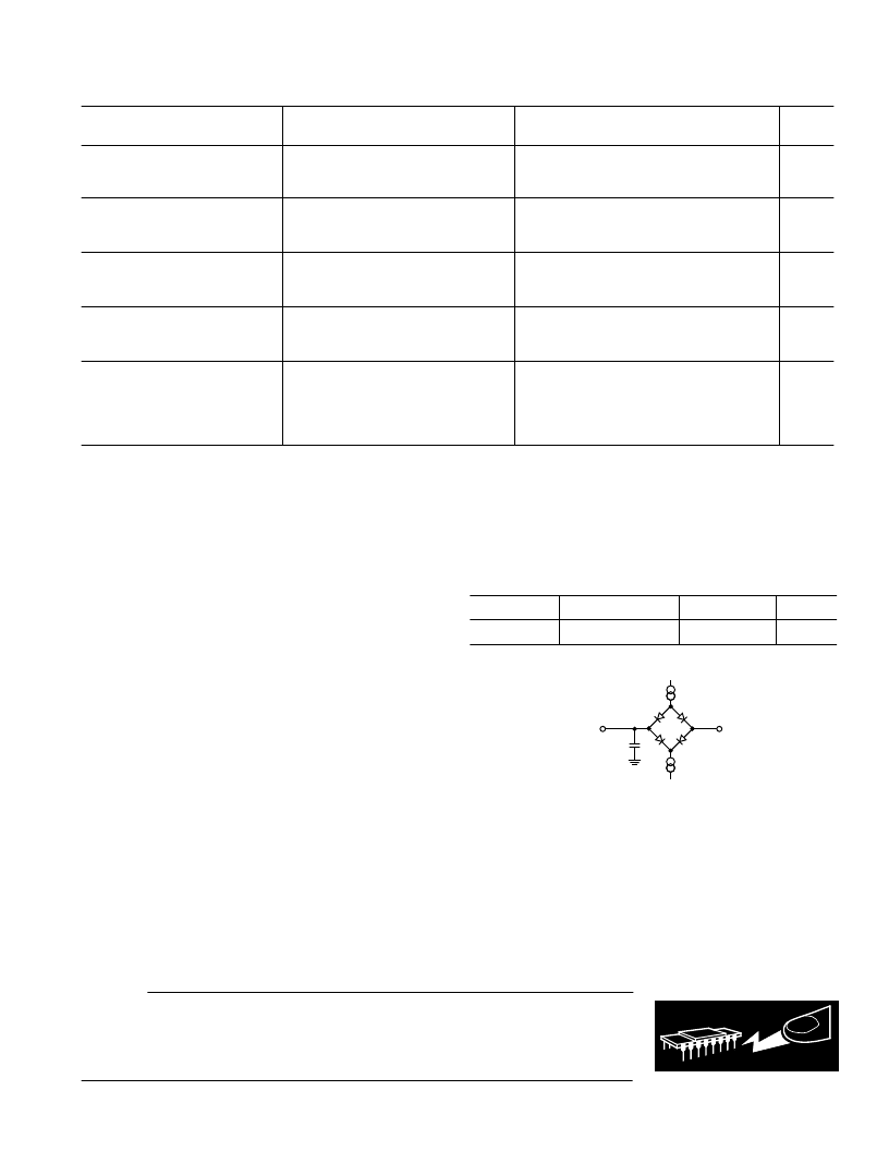
1.6mA
I
200μA
+1.6V
C
L
50pF
TO
OUTPUT
PIN
Figure 1. Load Circuit for Timing Specifications
相關PDF資料 |
PDF描述 |
|---|---|
| AD7722AS | 16-Bit, 195 kSPS CMOS, Sigma-Delta ADC |
| AD7723 | 16-Bit, 1.2 MSPS CMOS, Sigma-Delta ADC |
| AD7723BS | 16-Bit, 1.2 MSPS CMOS, Sigma-Delta ADC |
| AD7724AST | Dual CMOS Modulators |
| AD7724 | Dual CMOS Modulators |
相關代理商/技術參數 |
參數描述 |
|---|---|
| AD7722AS | 制造商:Rochester Electronics LLC 功能描述:16-BIT SIGMA-DELTA CONVERTER I.C. - Bulk 制造商:Analog Devices 功能描述:A/D Converter (A-D) IC |
| AD7722AS-ES | 制造商:Rochester Electronics LLC 功能描述:- Bulk |
| AD7722ASZ | 功能描述:IC ADC 16BIT 195KSPS 44-MQFP RoHS:是 類別:集成電路 (IC) >> 數據采集 - 模數轉換器 系列:- 標準包裝:1 系列:- 位數:14 采樣率(每秒):83k 數據接口:串行,并聯 轉換器數目:1 功率耗散(最大):95mW 電壓電源:雙 ± 工作溫度:0°C ~ 70°C 安裝類型:通孔 封裝/外殼:28-DIP(0.600",15.24mm) 供應商設備封裝:28-PDIP 包裝:管件 輸入數目和類型:1 個單端,雙極 |
| AD7722CSZ | 制造商:Analog Devices 功能描述: |
| AD7723 | 制造商:AD 制造商全稱:Analog Devices 功能描述:16-Bit, 1.2 MSPS CMOS, Sigma-Delta ADC |
發布緊急采購,3分鐘左右您將得到回復。