- 您現在的位置:買賣IC網 > PDF目錄373920 > AD7853LAR (ANALOG DEVICES INC) 3 V to 5 V Single Supply, 200 kSPS 12-Bit Sampling ADCs PDF資料下載
參數資料
| 型號: | AD7853LAR |
| 廠商: | ANALOG DEVICES INC |
| 元件分類: | ADC |
| 英文描述: | 3 V to 5 V Single Supply, 200 kSPS 12-Bit Sampling ADCs |
| 中文描述: | 1-CH 12-BIT SUCCESSIVE APPROXIMATION ADC, SERIAL ACCESS, PDSO24 |
| 封裝: | SOIC-24 |
| 文件頁數: | 12/34頁 |
| 文件大小: | 350K |
| 代理商: | AD7853LAR |
第1頁第2頁第3頁第4頁第5頁第6頁第7頁第8頁第9頁第10頁第11頁當前第12頁第13頁第14頁第15頁第16頁第17頁第18頁第19頁第20頁第21頁第22頁第23頁第24頁第25頁第26頁第27頁第28頁第29頁第30頁第31頁第32頁第33頁第34頁
REV. B
–12–
AD7853/AD7853L
CALIBRATION REGISTERS
The AD7853/AD7853L has ten calibration registers in all, eight for the DAC, one for the offset and one for gain. Data can be writ-
ten to or read from all ten calibration registers. In self- and system calibration the part automatically modifies the calibration regis-
ters; only if the user needs to modify the calibration registers should an attempt be made to read from and write to the calibration
registers.
Addressing the Calibration Registers
The calibration selection bits in the control register CALSLT1 and CALSLT0 determine which of the calibration registers are ad-
dressed (See Table IV). The addressing applies to both the read and write operations for the calibration registers. The user should
not attempt to read from and write to the calibration registers at the same time.
Table IV. Calibration Register Addressing
CALSLT1 CALSLT0
Comment
0
0
1
1
0
1
0
1
This combination addresses the
Gain (1)
,
Offset (1)
and
DAC Registers (8)
. Ten registers in total.
This combination addresses the
Gain (1)
and
Offset (1)
Registers. Two registers in total.
This combination addresses the
Offset Register
. One register in total.
This combination addresses the
Gain Register
. One register in total.
Writing to/Reading from the Calibration Registers
For writing to the calibration registers a write to the control
register is required to set the CALSLT0 and CALSLT1 bits.
For reading from the calibration registers a write to the control
register is required to set the CALSLT0 and CALSLT1 bits,
but also to set the RDSLT1 and RDSLT0 bits to 10 (this ad-
dresses the calibration registers for reading). The calibration
register pointer is reset on writing to the control register setting
the CALSLT1 and CALSLT0 bits, or upon completion of all
the calibration register write/read operations. When reset it
points to the first calibration register in the selected write/read
sequence. The calibration register pointer will point to the gain
calibration register upon reset in all but one case, this case
being where the offset calibration register is selected on its own
(CALSLT1 = 1, CALSLT0 = 0). Where more than one calibra-
tion register is being accessed, the calibration register pointer
will be automatically incremented after each calibration register
write/read operation. The order in which the ten calibration
registers are arranged is shown in Figure 7. The user may abort
at any time before all the calibration register write/read opera-
tions are completed, and the next control register write opera-
tion will reset the calibration register pointer. The flowchart in
Figure 8 shows the sequence for writing to the calibration regis-
ters and Figure 9 for reading.
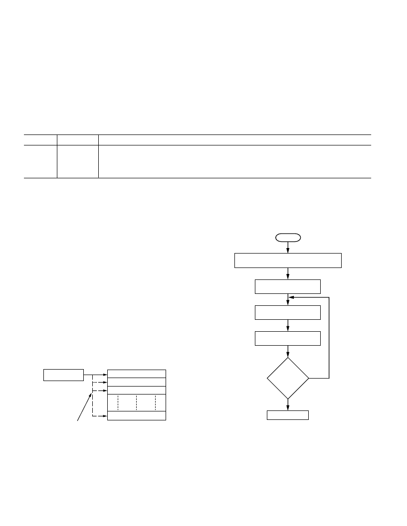
GAIN REGISTER
OFFSET REGISTER
DAC 1st MSB REGISTER
DAC 8th MSB REGISTER
CAL REGISTER
ADDRESS POINTER
CALIBRATION REGISTERS
(1)
(2)
(3)
(10)
CALIBRATION REGISTER ADDRESS POINTER POSITION IS
DETERMINED BY THE NUMBER OF CALIBRATION REGISTERS
ADDRESSED AND THE NUMBER OF READ/WRITE OPERATIONS.
Figure 7. Calibration Register Arrangement
When reading from the calibration registers there will always be
two leading zeros for each of the registers. When operating in
serial Interface Mode 1, the read operations to the calibration
registers cannot be aborted. The full number of read operations
must be completed (see section on serial Interface Mode 1 tim-
ing for more detail).
WRITE TO CONTROL REGISTER SETTING STCAL = 0
AND CALSLT1, CALSLT0 = 00, 01, 10, 11
CAL REGISTER POINTER IS
AUTOMATICALLY RESET
FINISHED
NO
YES
START
WRITE TO CAL REGISTER
(ADDR1 = 1, ADDR0 = 0)
CAL REGISTER POINTER IS
AUTOMATICALLY INCREMENTED
LAST
REGISTER
WRITE
OPERATION
OR
ABORT
Figure 8. Flowchart for Writing to the Calibration Registers
相關PDF資料 |
PDF描述 |
|---|---|
| AD7853LBN | 3 V to 5 V Single Supply, 200 kSPS 12-Bit Sampling ADCs |
| AD7853LBR | 3 V to 5 V Single Supply, 200 kSPS 12-Bit Sampling ADCs |
| AD7854LARS | 3 V to 5 V Single Supply, 200 kSPS 12-Bit Sampling ADCs |
| AD7854LAQ | 3 V to 5 V Single Supply, 200 kSPS 12-Bit Sampling ADCs |
| AD7854LAR | 3 V to 5 V Single Supply, 200 kSPS 12-Bit Sampling ADCs |
相關代理商/技術參數 |
參數描述 |
|---|---|
| AD7853LAR-REEL | 功能描述:IC ADC 12BIT SRL 200KSPS 24-SOIC RoHS:否 類別:集成電路 (IC) >> 數據采集 - 模數轉換器 系列:- 產品培訓模塊:Lead (SnPb) Finish for COTS Obsolescence Mitigation Program 標準包裝:2,500 系列:- 位數:12 采樣率(每秒):3M 數據接口:- 轉換器數目:- 功率耗散(最大):- 電壓電源:- 工作溫度:- 安裝類型:表面貼裝 封裝/外殼:SOT-23-6 供應商設備封裝:SOT-23-6 包裝:帶卷 (TR) 輸入數目和類型:- |
| AD7853LARS | 功能描述:IC ADC 12BIT SRL 200KSPS 24-SSOP RoHS:否 類別:集成電路 (IC) >> 數據采集 - 模數轉換器 系列:- 標準包裝:1,000 系列:- 位數:12 采樣率(每秒):300k 數據接口:并聯 轉換器數目:1 功率耗散(最大):75mW 電壓電源:單電源 工作溫度:0°C ~ 70°C 安裝類型:表面貼裝 封裝/外殼:24-SOIC(0.295",7.50mm 寬) 供應商設備封裝:24-SOIC 包裝:帶卷 (TR) 輸入數目和類型:1 個單端,單極;1 個單端,雙極 |
| AD7853LARS-REEL | 功能描述:IC ADC 12BIT SRL 200KSPS 24-SSOP RoHS:否 類別:集成電路 (IC) >> 數據采集 - 模數轉換器 系列:- 標準包裝:1,000 系列:- 位數:12 采樣率(每秒):300k 數據接口:并聯 轉換器數目:1 功率耗散(最大):75mW 電壓電源:單電源 工作溫度:0°C ~ 70°C 安裝類型:表面貼裝 封裝/外殼:24-SOIC(0.295",7.50mm 寬) 供應商設備封裝:24-SOIC 包裝:帶卷 (TR) 輸入數目和類型:1 個單端,單極;1 個單端,雙極 |
| AD7853LARSZ | 功能描述:IC ADC 12BIT SRL 200KSPS 24SSOP RoHS:是 類別:集成電路 (IC) >> 數據采集 - 模數轉換器 系列:- 標準包裝:1,000 系列:- 位數:12 采樣率(每秒):300k 數據接口:并聯 轉換器數目:1 功率耗散(最大):75mW 電壓電源:單電源 工作溫度:0°C ~ 70°C 安裝類型:表面貼裝 封裝/外殼:24-SOIC(0.295",7.50mm 寬) 供應商設備封裝:24-SOIC 包裝:帶卷 (TR) 輸入數目和類型:1 個單端,單極;1 個單端,雙極 |
| AD7853LARSZ-REEL | 功能描述:IC ADC 12BIT SRL 200KSPS 24SSOP RoHS:是 類別:集成電路 (IC) >> 數據采集 - 模數轉換器 系列:- 標準包裝:1,000 系列:- 位數:16 采樣率(每秒):45k 數據接口:串行 轉換器數目:2 功率耗散(最大):315mW 電壓電源:模擬和數字 工作溫度:0°C ~ 70°C 安裝類型:表面貼裝 封裝/外殼:28-SOIC(0.295",7.50mm 寬) 供應商設備封裝:28-SOIC W 包裝:帶卷 (TR) 輸入數目和類型:2 個單端,單極 |
發布緊急采購,3分鐘左右您將得到回復。