- 您現在的位置:買賣IC網 > PDF目錄373920 > AD7853LAR (ANALOG DEVICES INC) 3 V to 5 V Single Supply, 200 kSPS 12-Bit Sampling ADCs PDF資料下載
參數資料
| 型號: | AD7853LAR |
| 廠商: | ANALOG DEVICES INC |
| 元件分類: | ADC |
| 英文描述: | 3 V to 5 V Single Supply, 200 kSPS 12-Bit Sampling ADCs |
| 中文描述: | 1-CH 12-BIT SUCCESSIVE APPROXIMATION ADC, SERIAL ACCESS, PDSO24 |
| 封裝: | SOIC-24 |
| 文件頁數: | 21/34頁 |
| 文件大小: | 350K |
| 代理商: | AD7853LAR |
第1頁第2頁第3頁第4頁第5頁第6頁第7頁第8頁第9頁第10頁第11頁第12頁第13頁第14頁第15頁第16頁第17頁第18頁第19頁第20頁當前第21頁第22頁第23頁第24頁第25頁第26頁第27頁第28頁第29頁第30頁第31頁第32頁第33頁第34頁
REV. B
–21–
AD7853/AD7853L
capacitors, one of which is trimmed when an offset or gain cali-
bration is performed. Again it is the ratio of these capacitors to
the capacitors in the DAC that is critical and the calibration
algorithm ensures that this ratio is at a specified value for both
the offset and gain calibrations.
In Bipolar Mode the midscale error is adjusted for an offset
calibration and the positive full-scale error is adjusted for the
gain calibration; in Unipolar Mode the zero-scale error is ad-
justed for an offset calibration and the positive full-scale error is
adjusted for a gain calibration.
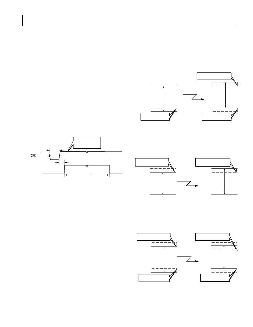
Self-Calibration Timing
The diagram of Figure 27 shows the timing for a full self-
calibration. Here the BUSY line stays high for the full length of
the self-calibration. A self-calibration is initiated by bringing the
CAL
pin low (which initiates an internal reset) and then high
again or by writing to the control register and setting the STCAL
bit to 1 (
note that if the part is in a power-down mode, the
CAL
pulsewidth must take account of the power-up time
). The BUSY line
is triggered high from the rising edge of
CAL
(or the end of the
write to the control register if calibration is initiated in soft-
ware), and BUSY will go low when the full self-calibration is
complete after a time t
CAL
as shown in Figure 27.
t
1
= 100ns MIN,
t
15
= 2.5
t
CLKIN
MAX,
t
CAL
= 125013
t
CLKIN
(I/P)
BUSY (O/P)
t
1
t
15
t
CAL
Figure 27. Timing Diagram for Full Self-Calibration
For the self-(gain + offset), self-offset and self-gain calibrations,
the BUSY line will be triggered high by the rising edge of the
CAL
signal (or the end of the write to the control register if
calibration is initiated in software) and will stay high for the full
duration of the self-calibration. The length of time that the
BUSY is high for will depend on the type of self-calibration that
is initiated. Typical figures are given in Table IX. The timing
diagrams for the other self-calibration options will be similar to
that outlined in Figure 27.
System Calibration Description
System calibration allows the user to take out system errors
external to the AD7853/AD7853L as well as calibrate the errors
of the AD7853/AD7853L itself. The maximum calibration
range for the system offset errors is
±
5% of V
REF
and for the
system gain errors is
±
2.5% of V
REF
. This means that the maxi-
mum allowable system offset voltage applied between the
AIN(+) and AIN(–) pins for the calibration to adjust out this
error is
±
0.05
×
V
REF
(
i.e., the AIN(+) can be 0.05
×
V
REF
above
AIN(–) or 0.05
×
V
REF
below AIN(–)
). For the system gain error
the maximum allowable system full-scale voltage, in unipolar
mode, that can be applied between AIN(+) and AIN(–) for the
calibration to adjust out this error is V
REF
±
0.025
×
V
REF
(
i.e.
,
the AIN(+) can be V
REF
+
0.025
×
V
REF
above AIN(–) or V
REF
–
0.025
×
V
REF
above AIN(–)
). If the system offset or system gain
errors are outside the ranges mentioned, the system calibration
algorithm will reduce the errors as much as the trim range allows.
Figures 33 through 35 illustrate why a specific type of system
calibration might be used. Figure 33 shows a system offset cali-
bration (assuming a positive offset) where the analog input
range has been shifted upwards by the system offset after the
system offset calibration is completed. A negative offset may
also be accounted for by a system offset calibration.
MAX SYSTEM FULL SCALE
IS
6
2.5% FROM V
REF
ANALOG
INPUT
RANGE
V
REF
– 1LSB
SYS OFFSET
AGND
MAX SYSTEM OFFSET
IS
6
5% OF V
REF
V
REF
+ SYS OFFSET
ANALOG
INPUT
RANGE
V
REF
– 1LSB
SYS OFFSET
AGND
MAX SYSTEM OFFSET
IS
6
5% OF V
REF
SYSTEM OFFSET
CALIBRATION
Figure 28. System Offset Calibration
Figure 29 shows a system gain calibration (assuming a system
full scale greater than the reference voltage) where the analog
input range has been increased after the system gain calibration
is completed. A system full-scale voltage less than the reference
voltage may also be accounted for a by a system gain calibration.
MAX SYSTEM FULL SCALE
IS
6
2.5% FROM V
REF
ANALOG
INPUT
RANGE
V
REF
– 1LSB
AGND
SYS FULL S.
ANALOG
INPUT
RANGE
V
REF
– 1LSB
SYS FULL S.
AGND
SYSTEM GAIN
CALIBRATION
MAX SYSTEM FULL SCALE
IS
6
2.5% FROM V
REF
Figure 29. System Gain Calibration
Finally in Figure 30 both the system offset and gain are ac-
counted for by the system offset followed by a system gain cali-
bration. First the analog input range is shifted upwards by the
positive system offset and then the analog input range is ad-
justed at the top end to account for the system full scale.
ANALOG
INPUT
RANGE
V
REF
– 1LSB
SYS OFFSET
AGND
V
REF
+ SYSSYS F.S.
ANALOG
INPUT
RANGE
V
REF
– 1LSB
SYS F. S.
AGND
SYSTEM OFFSET
CALIBRATION
FOLLOWED BY
SYSTEM GAIN
CALIBRATION
MAX SYSTEM FULL SCALE
IS
6
2.5% FROM V
REF
SYS OFFSET
MAX SYSTEM OFFSET
IS
6
5% OF V
REF
MAX SYSTEM OFFSET
IS
6
5% OF V
REF
MAX SYSTEM FULL SCALE
IS
6
2.5% FROM V
REF
Figure 30. System (Gain + Offset) Calibration
相關PDF資料 |
PDF描述 |
|---|---|
| AD7853LBN | 3 V to 5 V Single Supply, 200 kSPS 12-Bit Sampling ADCs |
| AD7853LBR | 3 V to 5 V Single Supply, 200 kSPS 12-Bit Sampling ADCs |
| AD7854LARS | 3 V to 5 V Single Supply, 200 kSPS 12-Bit Sampling ADCs |
| AD7854LAQ | 3 V to 5 V Single Supply, 200 kSPS 12-Bit Sampling ADCs |
| AD7854LAR | 3 V to 5 V Single Supply, 200 kSPS 12-Bit Sampling ADCs |
相關代理商/技術參數 |
參數描述 |
|---|---|
| AD7853LAR-REEL | 功能描述:IC ADC 12BIT SRL 200KSPS 24-SOIC RoHS:否 類別:集成電路 (IC) >> 數據采集 - 模數轉換器 系列:- 產品培訓模塊:Lead (SnPb) Finish for COTS Obsolescence Mitigation Program 標準包裝:2,500 系列:- 位數:12 采樣率(每秒):3M 數據接口:- 轉換器數目:- 功率耗散(最大):- 電壓電源:- 工作溫度:- 安裝類型:表面貼裝 封裝/外殼:SOT-23-6 供應商設備封裝:SOT-23-6 包裝:帶卷 (TR) 輸入數目和類型:- |
| AD7853LARS | 功能描述:IC ADC 12BIT SRL 200KSPS 24-SSOP RoHS:否 類別:集成電路 (IC) >> 數據采集 - 模數轉換器 系列:- 標準包裝:1,000 系列:- 位數:12 采樣率(每秒):300k 數據接口:并聯 轉換器數目:1 功率耗散(最大):75mW 電壓電源:單電源 工作溫度:0°C ~ 70°C 安裝類型:表面貼裝 封裝/外殼:24-SOIC(0.295",7.50mm 寬) 供應商設備封裝:24-SOIC 包裝:帶卷 (TR) 輸入數目和類型:1 個單端,單極;1 個單端,雙極 |
| AD7853LARS-REEL | 功能描述:IC ADC 12BIT SRL 200KSPS 24-SSOP RoHS:否 類別:集成電路 (IC) >> 數據采集 - 模數轉換器 系列:- 標準包裝:1,000 系列:- 位數:12 采樣率(每秒):300k 數據接口:并聯 轉換器數目:1 功率耗散(最大):75mW 電壓電源:單電源 工作溫度:0°C ~ 70°C 安裝類型:表面貼裝 封裝/外殼:24-SOIC(0.295",7.50mm 寬) 供應商設備封裝:24-SOIC 包裝:帶卷 (TR) 輸入數目和類型:1 個單端,單極;1 個單端,雙極 |
| AD7853LARSZ | 功能描述:IC ADC 12BIT SRL 200KSPS 24SSOP RoHS:是 類別:集成電路 (IC) >> 數據采集 - 模數轉換器 系列:- 標準包裝:1,000 系列:- 位數:12 采樣率(每秒):300k 數據接口:并聯 轉換器數目:1 功率耗散(最大):75mW 電壓電源:單電源 工作溫度:0°C ~ 70°C 安裝類型:表面貼裝 封裝/外殼:24-SOIC(0.295",7.50mm 寬) 供應商設備封裝:24-SOIC 包裝:帶卷 (TR) 輸入數目和類型:1 個單端,單極;1 個單端,雙極 |
| AD7853LARSZ-REEL | 功能描述:IC ADC 12BIT SRL 200KSPS 24SSOP RoHS:是 類別:集成電路 (IC) >> 數據采集 - 模數轉換器 系列:- 標準包裝:1,000 系列:- 位數:16 采樣率(每秒):45k 數據接口:串行 轉換器數目:2 功率耗散(最大):315mW 電壓電源:模擬和數字 工作溫度:0°C ~ 70°C 安裝類型:表面貼裝 封裝/外殼:28-SOIC(0.295",7.50mm 寬) 供應商設備封裝:28-SOIC W 包裝:帶卷 (TR) 輸入數目和類型:2 個單端,單極 |
發布緊急采購,3分鐘左右您將得到回復。