- 您現在的位置:買賣IC網 > PDF目錄373920 > AD7853LAR (ANALOG DEVICES INC) 3 V to 5 V Single Supply, 200 kSPS 12-Bit Sampling ADCs PDF資料下載
參數資料
| 型號: | AD7853LAR |
| 廠商: | ANALOG DEVICES INC |
| 元件分類: | ADC |
| 英文描述: | 3 V to 5 V Single Supply, 200 kSPS 12-Bit Sampling ADCs |
| 中文描述: | 1-CH 12-BIT SUCCESSIVE APPROXIMATION ADC, SERIAL ACCESS, PDSO24 |
| 封裝: | SOIC-24 |
| 文件頁數: | 9/34頁 |
| 文件大小: | 350K |
| 代理商: | AD7853LAR |
第1頁第2頁第3頁第4頁第5頁第6頁第7頁第8頁當前第9頁第10頁第11頁第12頁第13頁第14頁第15頁第16頁第17頁第18頁第19頁第20頁第21頁第22頁第23頁第24頁第25頁第26頁第27頁第28頁第29頁第30頁第31頁第32頁第33頁第34頁
REV. B
–9–
AD7853/AD7853L
ON-CHIP REGISTERS
The AD7853/AD7853L powers up with a set of default conditions, and the user need not ever write to the device. In this case the
AD7853/AD7853L will operate as a Read-Only ADC. The AD7853/AD7853L still retains the flexibility for performing a full power-
down, and a full self-calibration. Note that the DIN pin should be tied to DGND for operating the AD7853/AD7853L as a Read-
Only ADC.
Extra features and flexibility such as performing different power-down options, different types of calibrations including system cali-
bration, and software conversion start can be selected by writing to the part.
The AD7853/AD7853L contains a
Control register
,
ADC output data register
,
Status register
,
Test register
and
10 Calibra-
tion registers
. The control register is write-only, the ADC output data register and the status register are read-only, and the test and
calibration registers are both read/write registers. The test register is used for testing the part and should not be written to.
Addressing the On-Chip Registers
Writing
A write operation to the AD7853/AD7853L consists of 16 bits. The two MSBs, ADDR0 and ADDR1, are decoded to determine
which register is addressed, and the subsequent 14 bits of data are written to the addressed register. It is not until all 16 bits are writ-
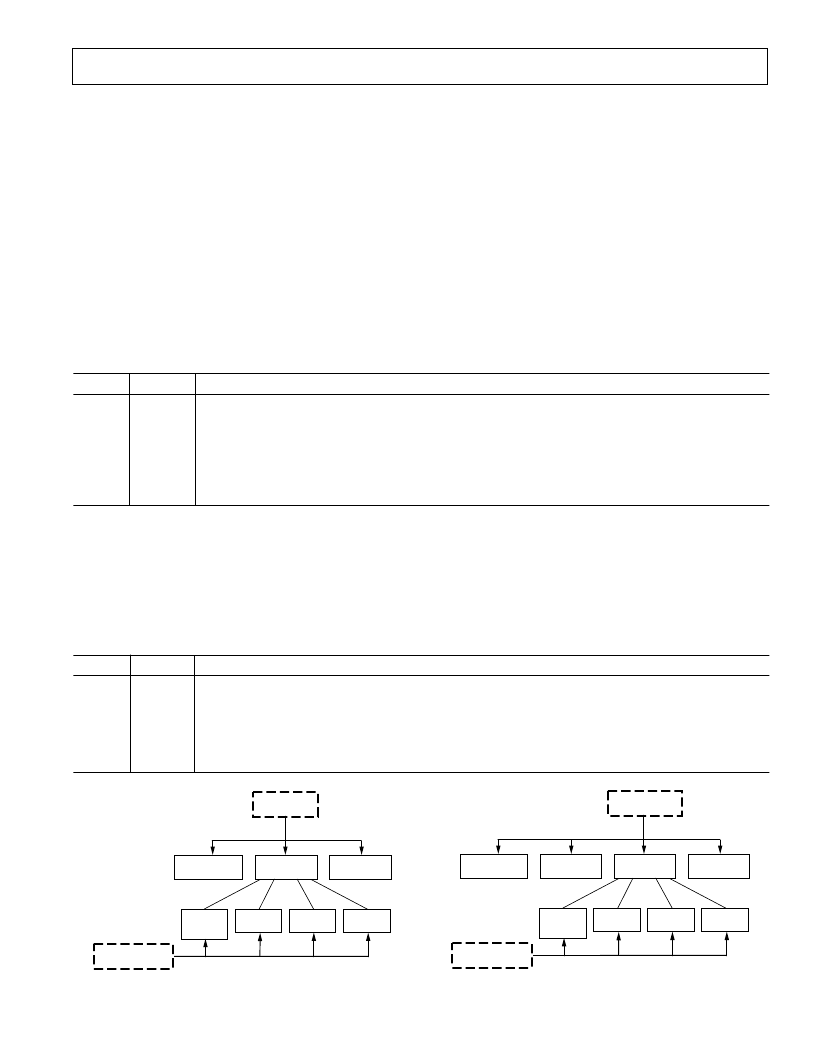
ten that the data is latched into the addressed register. Table I shows the decoding of the address bits, while Figure 4 shows the over-
all write register hierarchy.
Table I. Write Register Addressing
ADDR1
ADDR0
Comment
0
0
1
0
1
0
This combination does not address any register so the subsequent 14 data bits are ignored.
This combination addresses the
TEST REGISTER
. The subsequent 14 data bits are written to the test register.
This combination addresses the
CALIBRATION REGISTERS
. The subsequent 14 data bits are written
to the selected calibration register.
This combination addresses the
CONTROL REGISTER
. The subsequent 14 data bits are written to the
control register.
1
1
Reading
To read from the various registers the user must first write to Bits 6 and 7 in the Control Register, RDSLT0 and RDSLT1. These
bits are decoded to determine which register is addressed during a read operation. Table II shows the decoding of the read address
bits while Figure 5 shows the overall read register hierarchy. The power-up status of these bits is 00 so that the default read will be
from the ADC output data register.
Once the read selection bits are set in the control register all subsequent read operations that follow will be from the selected register
until the read selection bits are changed in the control register.
Table II. Read Register Addressing
RDSLT1
RDSLT0
Comment
0
0
All successive read operations will be from
ADC OUTPUT DATA REGISTER
. This is the power-up
default setting. There will always be four leading zeros when reading from the ADC output data register.
All successive read operations will be from
TEST REGISTER
.
All successive read operations will be from
CALIBRATION REGISTERS
.
All successive read operations will be from
STATUS REGISTER
.
0
1
1
1
0
1
ADDR1, ADDR0
DECODE
CALIBRATION
REGISTERS
GAIN(1)
OFFSET(1)
01
10
11
CALSLT1, CALSLT0
DECODE
00
01
10
11
TEST
REGISTER
CONTROL
REGISTER
OFFSET(1)
GAIN(1)
GAIN(1)
OFFSET(1)
DAC(8)
Figure 4. Write Register Hierarchy/Address Decoding
RDSLT1, RDSLT0
DECODE
CALIBRATION
REGISTERS
GAIN(1)
OFFSET(1)
01
10
11
CALSLT1, CALSLT0
DECODE
00
01
10
11
TEST
REGISTER
STATUS
REGISTER
OFFSET(1)
GAIN(1)
GAIN(1)
OFFSET(1)
DAC(8)
ADC OUTPUT
DATA REGISTER
00
Figure 5. Read Register Hierarchy/Address Decoding
相關PDF資料 |
PDF描述 |
|---|---|
| AD7853LBN | 3 V to 5 V Single Supply, 200 kSPS 12-Bit Sampling ADCs |
| AD7853LBR | 3 V to 5 V Single Supply, 200 kSPS 12-Bit Sampling ADCs |
| AD7854LARS | 3 V to 5 V Single Supply, 200 kSPS 12-Bit Sampling ADCs |
| AD7854LAQ | 3 V to 5 V Single Supply, 200 kSPS 12-Bit Sampling ADCs |
| AD7854LAR | 3 V to 5 V Single Supply, 200 kSPS 12-Bit Sampling ADCs |
相關代理商/技術參數 |
參數描述 |
|---|---|
| AD7853LAR-REEL | 功能描述:IC ADC 12BIT SRL 200KSPS 24-SOIC RoHS:否 類別:集成電路 (IC) >> 數據采集 - 模數轉換器 系列:- 產品培訓模塊:Lead (SnPb) Finish for COTS Obsolescence Mitigation Program 標準包裝:2,500 系列:- 位數:12 采樣率(每秒):3M 數據接口:- 轉換器數目:- 功率耗散(最大):- 電壓電源:- 工作溫度:- 安裝類型:表面貼裝 封裝/外殼:SOT-23-6 供應商設備封裝:SOT-23-6 包裝:帶卷 (TR) 輸入數目和類型:- |
| AD7853LARS | 功能描述:IC ADC 12BIT SRL 200KSPS 24-SSOP RoHS:否 類別:集成電路 (IC) >> 數據采集 - 模數轉換器 系列:- 標準包裝:1,000 系列:- 位數:12 采樣率(每秒):300k 數據接口:并聯 轉換器數目:1 功率耗散(最大):75mW 電壓電源:單電源 工作溫度:0°C ~ 70°C 安裝類型:表面貼裝 封裝/外殼:24-SOIC(0.295",7.50mm 寬) 供應商設備封裝:24-SOIC 包裝:帶卷 (TR) 輸入數目和類型:1 個單端,單極;1 個單端,雙極 |
| AD7853LARS-REEL | 功能描述:IC ADC 12BIT SRL 200KSPS 24-SSOP RoHS:否 類別:集成電路 (IC) >> 數據采集 - 模數轉換器 系列:- 標準包裝:1,000 系列:- 位數:12 采樣率(每秒):300k 數據接口:并聯 轉換器數目:1 功率耗散(最大):75mW 電壓電源:單電源 工作溫度:0°C ~ 70°C 安裝類型:表面貼裝 封裝/外殼:24-SOIC(0.295",7.50mm 寬) 供應商設備封裝:24-SOIC 包裝:帶卷 (TR) 輸入數目和類型:1 個單端,單極;1 個單端,雙極 |
| AD7853LARSZ | 功能描述:IC ADC 12BIT SRL 200KSPS 24SSOP RoHS:是 類別:集成電路 (IC) >> 數據采集 - 模數轉換器 系列:- 標準包裝:1,000 系列:- 位數:12 采樣率(每秒):300k 數據接口:并聯 轉換器數目:1 功率耗散(最大):75mW 電壓電源:單電源 工作溫度:0°C ~ 70°C 安裝類型:表面貼裝 封裝/外殼:24-SOIC(0.295",7.50mm 寬) 供應商設備封裝:24-SOIC 包裝:帶卷 (TR) 輸入數目和類型:1 個單端,單極;1 個單端,雙極 |
| AD7853LARSZ-REEL | 功能描述:IC ADC 12BIT SRL 200KSPS 24SSOP RoHS:是 類別:集成電路 (IC) >> 數據采集 - 模數轉換器 系列:- 標準包裝:1,000 系列:- 位數:16 采樣率(每秒):45k 數據接口:串行 轉換器數目:2 功率耗散(最大):315mW 電壓電源:模擬和數字 工作溫度:0°C ~ 70°C 安裝類型:表面貼裝 封裝/外殼:28-SOIC(0.295",7.50mm 寬) 供應商設備封裝:28-SOIC W 包裝:帶卷 (TR) 輸入數目和類型:2 個單端,單極 |
發布緊急采購,3分鐘左右您將得到回復。