- 您現在的位置:買賣IC網 > PDF目錄373969 > AD9848 (Analog Devices, Inc.) CCD Signal Processors with Integrated Timing Driver PDF資料下載
參數資料
| 型號: | AD9848 |
| 廠商: | Analog Devices, Inc. |
| 英文描述: | CCD Signal Processors with Integrated Timing Driver |
| 中文描述: | CCD信號處理器集成時序驅動 |
| 文件頁數: | 20/36頁 |
| 文件大小: | 347K |
| 代理商: | AD9848 |
第1頁第2頁第3頁第4頁第5頁第6頁第7頁第8頁第9頁第10頁第11頁第12頁第13頁第14頁第15頁第16頁第17頁第18頁第19頁當前第20頁第21頁第22頁第23頁第24頁第25頁第26頁第27頁第28頁第29頁第30頁第31頁第32頁第33頁第34頁第35頁第36頁
REV. 0
AD9848/AD9849
–20–
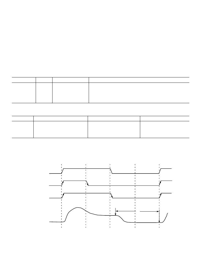
H-Driver and RG Outputs
In addition to the programmable timing positions, the AD9848/
AD9849 features on-chip output drivers for the RG and H1–H4
outputs. These drivers are powerful enough to directly drive the
CCD inputs. The H-driver current can be adjusted for optimum
rise/fall time into a particular load by using the DRV registers. The
RG drive current is adjustable using the RGDRV register. Each
3-bit DRV register is adjustable in 3.5 mA increments, with the
minimum setting of 0 equal to OFF or three-state, and the maxi-
mum setting of 7 equal to 24.5 mA.
As shown in Figure 7, the H2/H4 outputs are inverses of H1/
H3. The internal propagation delay resulting from the signal
inversion is less than l ns, which is significantly less than the
typical rise time driving the CCD load. This results in a H1/H2
crossover voltage at approximately 50% of the output swing.
The crossover voltage is not programmable.
Digital Data Outputs
The AD9848/AD9849 data output phase is programmable
using the DOUTPHASE register. Any edge from 0 to 47 may
be programmed, as shown in Figure 8.
P[0]
PIXEL
PERIOD
RG
H1/H3
RGf[12]
P[48] = P[0]
Hf[24]
SHP[28]
CCD SIGNAL
P[24]
P[12]
P[36]
Hr[0]
RGr[0]
SHD[48]
NOTES
1. ALL SIGNAL EDGES ARE FULLY PROGRAMMABLE TO ANY OF THE 48 POSITIONS WITHIN ONE PIXEL PERIOD.
2. DEFAULT POSITIONS FOR EACH SIGNAL ARE SHOWN ABOVE.
POSITION
t
S1
Figure 6. High-Speed Clock Default and Programmable Locations
Table II. H1–H4, RG, SHP, SHD Timing Parameters
Register Name
Length
Range
Description
POL
POSLOC
1b
6b
High/Low
0–47 Edge Location
Polarity Control for H1, H3, and RG (0 = No Inversion, 1 = Inversion)
Positive Edge Location for H1, H3, and RG
Sample Location for SHP, SHD
Negative Edge Location for H1, H3, and RG
Drive Current for H1–H4 and RG Outputs (3.5 mA Per Step)
NEGLOC
DRV
6b
3b
0–47 Edge Location
0–7 Current Steps
Table III.
Precision Timing
Edge Locations
Quadrant
Edge Location (Decimal)
Register Value (Decimal)
Register Value (Binary)
I
II
III
IV
0 to 11
12 to 23
24 to 35
36 to 47
0 to 11
16 to 27
32 to 43
48 to 59
000000 to 001011
010000 to 011011
100000 to 101011
110000 to 111011
相關PDF資料 |
PDF描述 |
|---|---|
| AD9849 | CCD Signal Processors with Integrated Timing Driver |
| AD9849KST | CCD Signal Processors with Integrated Timing Driver |
| AD9851 | CMOS 180 MHz DDS/DAC Synthesizer |
| AD9852 | CMOS 300MHz Complete-DDS Synthesizer |
| AD9853 | Programmable Digital QPSK/16-QAM Modulator(可編程數字的四相移鍵控/16-正交幅度調制的調節器) |
相關代理商/技術參數 |
參數描述 |
|---|---|
| AD9848AKST | 制造商:Analog Devices 功能描述:AFE Video 1ADC 10-Bit 3V/3.3V 48-Pin LQFP 制造商:Analog Devices 功能描述:AFE VID 1ADC 10-BIT 3V/3V/3.3V/3.3V/3.3V/3.3V/3.3V 48LQFP - Bulk 制造商:Rochester Electronics LLC 功能描述:10 BIT 20 MSPS CCD SIGNAL PROCESSOR - Tape and Reel |
| AD9848AKSTRL | 制造商:Analog Devices 功能描述:AFE Video 1ADC 10-Bit 3V/3.3V 48-Pin LQFP T/R 制造商:Analog Devices 功能描述:AFE VID 1ADC 10-BIT 3V/3V/3.3V/3.3V/3.3V/3.3V/3.3V 48LQFP - Tape and Reel |
| AD9848AKSTZ | 制造商:Analog Devices 功能描述: |
| AD9848AKSTZRL | 制造商:Analog Devices 功能描述: |
| AD9848KST | 制造商:Rochester Electronics LLC 功能描述:10 BIT 18 MSPS 3V AFE & T - Bulk |
發布緊急采購,3分鐘左右您將得到回復。