- 您現在的位置:買賣IC網 > PDF目錄373969 > AD9851 (Analog Devices, Inc.) CMOS 180 MHz DDS/DAC Synthesizer PDF資料下載
參數資料
| 型號: | AD9851 |
| 廠商: | Analog Devices, Inc. |
| 元件分類: | XO, clock |
| 英文描述: | CMOS 180 MHz DDS/DAC Synthesizer |
| 中文描述: | 180MHz的CMOS/DAC頻率合成器 |
| 文件頁數: | 1/23頁 |
| 文件大小: | 277K |
| 代理商: | AD9851 |
REV. 0
Information furnished by Analog Devices is believed to be accurate and
reliable. However, no responsibility is assumed by Analog Devices for its
use, nor for any infringements of patents or other rights of third parties
which may result from its use. No license is granted by implication or
otherwise under any patent or patent rights of Analog Devices.
a
AD9851
One Technology Way, P.O. Box 9106, Norwood, MA 02062-9106, U.S.A.
Tel: 781/329-4700
World Wide Web Site: http://www.analog.com
Fax: 781/326-8703
Analog Devices, Inc., 1998
CMOS 180 MHz
DDS/DAC Synthesizer
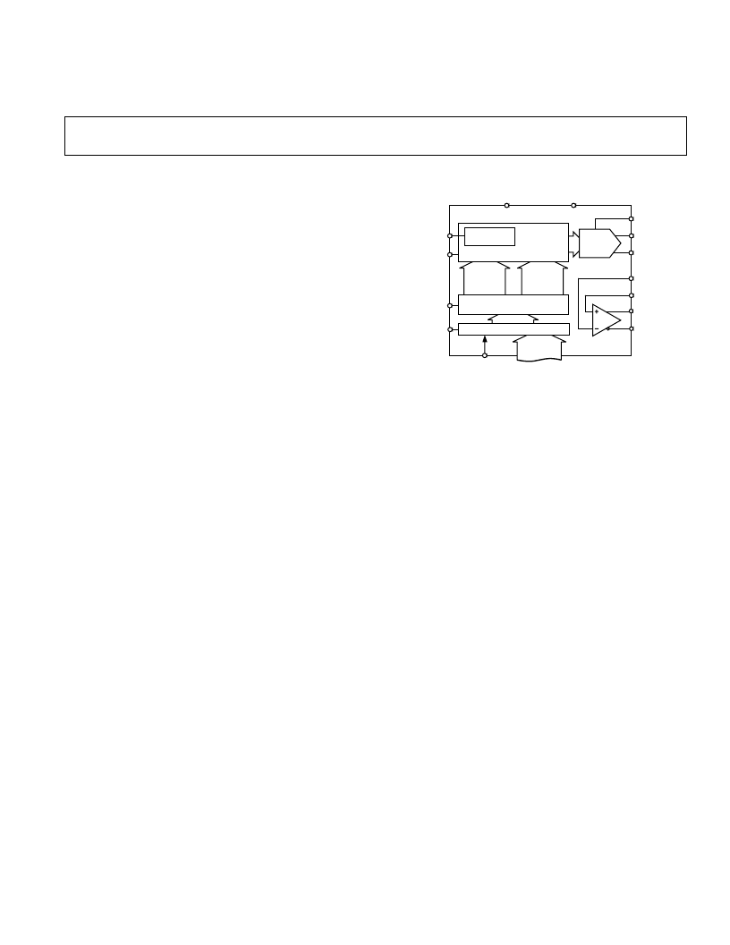
FUNCTIONAL BLOCK DIAGRAM
32-BIT
TUNING
WORD
PHASE
AND
CONTROL
WORDS
FREQUENCY/PHASE
DATA REGISTER
DATA INPUT REGISTER
SERIAL
LOAD
10-BIT
DAC
DAC R
SET
ANALOG
OUT
ANALOG
IN
CLOCK OUT
CLOCK
OUT
HIGH SPEED
DDS
FREQUENCY
UPDATE/DATA
REGISTER
RESET
WORD LOAD
CLOCK
MASTER
RESET
REF
CLOCK IN
6
REFCLK
MULTIPLIER
COMPARATOR
1 BIT
40 LOADS
PARALLEL
LOAD
8 BITS
3
5 LOADS
FREQUENCY, PHASE
AND CONTROL DATA INPUT
AD9851
+V
S
GND
FEATURES
180 MHz Clock Rate with Selectable 6
3
Reference Clock
Multiplier
On-Chip High Performance 10-Bit DAC and High Speed
Comparator with Hysteresis
SFDR >43 dB @ 70 MHz A
OUT
32-Bit Frequency Tuning Word
Simplified Control Interface: Parallel or Serial
Asynchronous Loading Format
5-Bit Phase Modulation and Offset Capability
Comparator Jitter <80 ps p-p @ 20 MHz
+2.7 V to +5.25 V Single Supply Operation
Low Power: 555 mW @ 180 MHz
Power-Down Function, 4 mW @ +2.7 V
Ultrasmall 28-Lead SSOP Packaging
APPLICATIONS
Frequency/Phase-Agile Sine Wave Synthesis
Clock Recovery and Locking Circuitry for Digital
Communications
Digitally Controlled ADC Encode Generator
Agile L.O. Applications in Communications
Quadrature Oscillator
CW, AM, FM, FSK, MSK Mode Transmitter
GENERAL DESCRIPTION
The AD9851 is a highly integrated device that uses advanced
DDS technology, coupled with an internal high speed, high
performance D/A converter, and comparator, to form a digitally-
programmable frequency synthesizer and clock generator func-
tion. When referenced to an accurate clock source, the AD9851
generates a stable frequency and phase-programmable digitized
analog output sine wave. This sine wave can be used directly as
a frequency source, or internally converted to a square wave for
agile-clock generator applications. The AD9851’s innovative
high speed DDS core accepts a 32-bit frequency tuning word,
which results in an output tuning resolution of approximately
0.04 Hz with a 180 MHz system clock. The AD9851 contains a
unique 6
×
REFCLK Multiplier circuit that eliminates the need
for a high speed reference oscillator. The 6
×
REFCLK Multiplier
has minimal impact on SFDR and phase noise characteristics.
The AD9851 provides five bits of programmable phase modula-
tion resolution to enable phase shifting of its output in incre-
ments of 11.25
°
.
The AD9851 contains an internal high speed comparator that
can be configured to accept the (externally) filtered output of
the DAC to generate a low jitter output pulse.
The frequency tuning, control and phase modulation words are
asynchronously loaded into the AD9851 via parallel or serial
loading format. The parallel load format consists of five itera-
tive loads of an 8-bit control word (byte). The first 8-bit byte
controls output phase, 6
×
REFCLK Multiplier, power-down
enable and loading format; the remaining bytes comprise the
32-bit frequency tuning word. Serial loading is accomplished
via a 40-bit serial data stream entering through one of the parallel
input bus lines. The AD9851 uses advanced CMOS technology
to provide this breakthrough level of functionality on just 555 mW
of power dissipation (+5 V supply), at the maximum clock rate of
180 MHz.
The AD9851 is available in a space-saving 28-lead SSOP, sur-
face mount package that is pin-for-pin compatible with the
popular AD9850 125 MHz DDS. It is specified to operate over
the extended industrial temperature range of –40
°
C to +85
°
C.
相關PDF資料 |
PDF描述 |
|---|---|
| AD9852 | CMOS 300MHz Complete-DDS Synthesizer |
| AD9853 | Programmable Digital QPSK/16-QAM Modulator(可編程數字的四相移鍵控/16-正交幅度調制的調節器) |
| AD9854 | CMOS 300MHz Quadrature Complete-DDS |
| AD9858TLPCB | 1 GSPS Direct Digital Synthesizer |
| AD9858BSV | 1 GSPS Direct Digital Synthesizer |
相關代理商/技術參數 |
參數描述 |
|---|---|
| AD9851/CGPCB | 制造商:Analog Devices 功能描述:NCO/DDS, CMOS 180MHZ DDS/DAC SYNTHESIZER - Bulk 制造商:Rochester Electronics LLC 功能描述:DDS CLOCK DRIVER - Bulk |
| AD9851/FSPCB | 制造商:Analog Devices 功能描述:Evaluation Board For NCO/DDS, CMOS 180MHZ DDS/DAC Synthesizer 制造商:Analog Devices 功能描述:NCO/DDS, CMOS 180MHZ DDS/DAC SYNTHESIZER - Bulk |
| AD9851BRS | 功能描述:IC DDS DAC W/COMP 180MHZ 28-SSOP RoHS:否 類別:集成電路 (IC) >> 接口 - 直接數字合成 (DDS) 系列:- 產品變化通告:Product Discontinuance 27/Oct/2011 標準包裝:2,500 系列:- 分辨率(位):10 b 主 fclk:25MHz 調節字寬(位):32 b 電源電壓:2.97 V ~ 5.5 V 工作溫度:-40°C ~ 85°C 安裝類型:表面貼裝 封裝/外殼:16-TSSOP(0.173",4.40mm 寬) 供應商設備封裝:16-TSSOP 包裝:帶卷 (TR) |
| AD9851BRSRL | 功能描述:IC DDS/DAC SYNTHESIZER 28-SSOP RoHS:否 類別:集成電路 (IC) >> 接口 - 直接數字合成 (DDS) 系列:- 產品變化通告:Product Discontinuance 27/Oct/2011 標準包裝:2,500 系列:- 分辨率(位):10 b 主 fclk:25MHz 調節字寬(位):32 b 電源電壓:2.97 V ~ 5.5 V 工作溫度:-40°C ~ 85°C 安裝類型:表面貼裝 封裝/外殼:16-TSSOP(0.173",4.40mm 寬) 供應商設備封裝:16-TSSOP 包裝:帶卷 (TR) |
| AD9851BRSZ | 功能描述:IC SYNTHESIZER DDS/DAC 28-SSOP RoHS:是 類別:集成電路 (IC) >> 接口 - 直接數字合成 (DDS) 系列:- 產品變化通告:Product Discontinuance 27/Oct/2011 標準包裝:2,500 系列:- 分辨率(位):10 b 主 fclk:25MHz 調節字寬(位):32 b 電源電壓:2.97 V ~ 5.5 V 工作溫度:-40°C ~ 85°C 安裝類型:表面貼裝 封裝/外殼:16-TSSOP(0.173",4.40mm 寬) 供應商設備封裝:16-TSSOP 包裝:帶卷 (TR) |
發布緊急采購,3分鐘左右您將得到回復。