- 您現(xiàn)在的位置:買賣IC網(wǎng) > PDF目錄373969 > AD9851 (Analog Devices, Inc.) CMOS 180 MHz DDS/DAC Synthesizer PDF資料下載
參數(shù)資料
| 型號: | AD9851 |
| 廠商: | Analog Devices, Inc. |
| 元件分類: | XO, clock |
| 英文描述: | CMOS 180 MHz DDS/DAC Synthesizer |
| 中文描述: | 180MHz的CMOS/DAC頻率合成器 |
| 文件頁數(shù): | 8/23頁 |
| 文件大小: | 277K |
| 代理商: | AD9851 |
AD9851
–8–
REV. 0
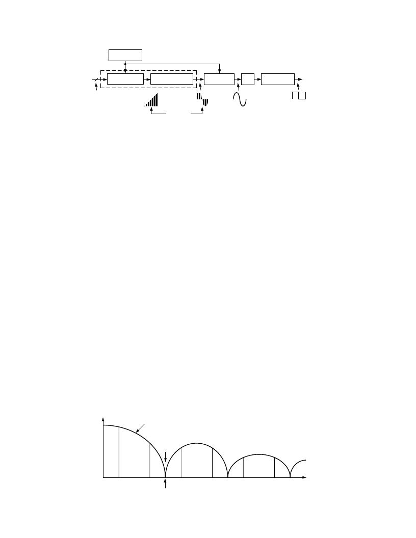
THEORY OF OPERATION AND APPLICATION
The AD9851 uses direct digital synthesis (DDS) technology, in
the form of a numerically-controlled oscillator (NCO), to gen-
erate a frequency/phase-agile sine wave. The digital sine wave is
converted to analog form via an internal 10-bit high speed D/A
converter. An on-board high-speed comparator is provided to
translate the analog sine wave into a low-jitter TTL/CMOS-
compatible output square wave. DDS technology is an innova-
tive circuit architecture that allows fast and precise manipulation
of its output word, under full digital control. DDS also enables
very high resolution in the incremental selection of output fre-
quency. The AD9851 allows an output frequency resolution of
approximately 0.04 Hz at 180 MSPS clock rate with the option of
directly using the reference clock or by engaging the 6
×
REFCLK
Multiplier. The AD9851’s output waveform is phase-continu-
ous from one output frequency change to another.
The basic functional block diagram and signal flow of the
AD9851 configured as a clock generator is shown in Figure 11.
The DDS circuitry is basically a digital frequency divider func-
tion whose incremental resolution is determined by the frequency
of the system clock, and N (number of bits in the tuning word).
The phase accumulator is a variable-modulus counter that
increments the number stored in it each time it receives a clock
pulse. When the counter reaches full scale it “wraps around,”
making the phase accumulator’s output phase-continuous. The
frequency tuning word sets the modulus of the counter, which
effectively determines the size of the increment (
Phase) that
will be added to the value in the phase accumulator on the next
clock pulse. The larger the added increment, the faster the
accumulator wraps around, which results in a higher output
frequency.
The AD9851 uses an innovative and proprietary “Angle
Rotation” algorithm that mathematically converts the 14-bit
truncated value of the 32-bit phase accumulator to the 10-bit
quantized amplitude that is passed to the DAC. This unique
algorithm uses a much-reduced ROM look-up table and DSP to
perform this function. This contributes to the small size and
low power dissipation of the AD9851.
The relationship between the output frequency, system clock
and tuning word of the AD9851 is determined by the expression:
f
OUT
= (
Phase
×
System Clock)/
2
32
where:
Phase
= decimal value of 32-bit frequency tuning word.
System Clock
= direct input reference clock (in MHz) or 6
×
the
input clock (in MHz) if the 6
×
REFCLK Multiplier is engaged.
f
OUT
= frequency of the output signal in MHz.
The digital sine wave output of the DDS core drives the internal
high-speed 10-bit D/A converter that will construct the sine
wave in analog form. This DAC has been optimized for dynamic
performance and low glitch energy, which results in the low
spurious and jitter performance of the AD9851. The DAC can
be operated in either the single-ended, Figures 2 and 8, or dif-
ferential output configuration, Figures 9 and 10. DAC output
current and R
SET
values are determined using the following
expressions:
I
OUT
= 39.93/
R
SET
R
SET
= 39.93/
I
OUT
Since the output of the AD9851 is a sampled signal, its output
spectrum follows the Nyquist sampling theorem. Specifically, its
output spectrum contains the fundamental plus aliased signals
(images) that occur at integer multiples of the system clock
frequency
±
the selected output frequency. A graphical repre-
sentation of the sampled spectrum, with aliased images, is shown in
Figure 12. Normal usable bandwidth is considered to extend
from dc to 1/2 the system clock.
In the example shown in Figure 12, the system clock is 100 MHz
and the output frequency is set to 20 MHz. As can be seen, the
aliased images are very prominent and of a relatively high energy
CLOCK
OUT
AMPLITUDE/SINE
CONV ALGORITHM
PHASE
ACCUMULATOR
DDS CIRCUITRY
D/A
CONVERTER
LP
COMPARATOR
N
REFERENCE
CLOCK
TUNING WORD SPECIFIES
OUTPUT FREQUENCY AS A
FRACTION OF REF CLOCK
FREQUENCY
IN DIGITAL
DOMAIN
Figure 11. Basic DDS Block Diagram and Signal Flow of AD9851
120MHz
2ND IMAGE
F
OUT
F
C
+F
O
2F
C
–F
O
2F
C
+F
O
3F
C
–F
O
180MHz
3RD IMAGE
220MHz
4TH IMAGE
280MHz
5TH IMAGE
80MHz
1ST IMAGE
20MHz
0Hz
(DC)
F
C
F
C
–F
O
SIN (X)/
3
ENVELOPE
3
= (
p
)F/F
C
100MHz
SYSTEM CLOCK FREQUENCY
S
Figure 12. Output Spectrum of a Sampled Sin(X)/X Signal
相關(guān)PDF資料 |
PDF描述 |
|---|---|
| AD9852 | CMOS 300MHz Complete-DDS Synthesizer |
| AD9853 | Programmable Digital QPSK/16-QAM Modulator(可編程數(shù)字的四相移鍵控/16-正交幅度調(diào)制的調(diào)節(jié)器) |
| AD9854 | CMOS 300MHz Quadrature Complete-DDS |
| AD9858TLPCB | 1 GSPS Direct Digital Synthesizer |
| AD9858BSV | 1 GSPS Direct Digital Synthesizer |
相關(guān)代理商/技術(shù)參數(shù) |
參數(shù)描述 |
|---|---|
| AD9851/CGPCB | 制造商:Analog Devices 功能描述:NCO/DDS, CMOS 180MHZ DDS/DAC SYNTHESIZER - Bulk 制造商:Rochester Electronics LLC 功能描述:DDS CLOCK DRIVER - Bulk |
| AD9851/FSPCB | 制造商:Analog Devices 功能描述:Evaluation Board For NCO/DDS, CMOS 180MHZ DDS/DAC Synthesizer 制造商:Analog Devices 功能描述:NCO/DDS, CMOS 180MHZ DDS/DAC SYNTHESIZER - Bulk |
| AD9851BRS | 功能描述:IC DDS DAC W/COMP 180MHZ 28-SSOP RoHS:否 類別:集成電路 (IC) >> 接口 - 直接數(shù)字合成 (DDS) 系列:- 產(chǎn)品變化通告:Product Discontinuance 27/Oct/2011 標(biāo)準(zhǔn)包裝:2,500 系列:- 分辨率(位):10 b 主 fclk:25MHz 調(diào)節(jié)字寬(位):32 b 電源電壓:2.97 V ~ 5.5 V 工作溫度:-40°C ~ 85°C 安裝類型:表面貼裝 封裝/外殼:16-TSSOP(0.173",4.40mm 寬) 供應(yīng)商設(shè)備封裝:16-TSSOP 包裝:帶卷 (TR) |
| AD9851BRSRL | 功能描述:IC DDS/DAC SYNTHESIZER 28-SSOP RoHS:否 類別:集成電路 (IC) >> 接口 - 直接數(shù)字合成 (DDS) 系列:- 產(chǎn)品變化通告:Product Discontinuance 27/Oct/2011 標(biāo)準(zhǔn)包裝:2,500 系列:- 分辨率(位):10 b 主 fclk:25MHz 調(diào)節(jié)字寬(位):32 b 電源電壓:2.97 V ~ 5.5 V 工作溫度:-40°C ~ 85°C 安裝類型:表面貼裝 封裝/外殼:16-TSSOP(0.173",4.40mm 寬) 供應(yīng)商設(shè)備封裝:16-TSSOP 包裝:帶卷 (TR) |
| AD9851BRSZ | 功能描述:IC SYNTHESIZER DDS/DAC 28-SSOP RoHS:是 類別:集成電路 (IC) >> 接口 - 直接數(shù)字合成 (DDS) 系列:- 產(chǎn)品變化通告:Product Discontinuance 27/Oct/2011 標(biāo)準(zhǔn)包裝:2,500 系列:- 分辨率(位):10 b 主 fclk:25MHz 調(diào)節(jié)字寬(位):32 b 電源電壓:2.97 V ~ 5.5 V 工作溫度:-40°C ~ 85°C 安裝類型:表面貼裝 封裝/外殼:16-TSSOP(0.173",4.40mm 寬) 供應(yīng)商設(shè)備封裝:16-TSSOP 包裝:帶卷 (TR) |
發(fā)布緊急采購,3分鐘左右您將得到回復(fù)。