- 您現在的位置:買賣IC網 > PDF目錄373969 > AD9859 (Analog Devices, Inc.) 400 MSPS, 10-Bit, 1.8 V CMOS Direct Digital Synthesizer PDF資料下載
參數資料
| 型號: | AD9859 |
| 廠商: | Analog Devices, Inc. |
| 元件分類: | XO, clock |
| 英文描述: | 400 MSPS, 10-Bit, 1.8 V CMOS Direct Digital Synthesizer |
| 中文描述: | 400 MSPS的10位,1.8伏的CMOS直接數字頻率合成 |
| 文件頁數: | 19/24頁 |
| 文件大小: | 574K |
| 代理商: | AD9859 |
AD9859
Rev. 0 | Page 19 of 24
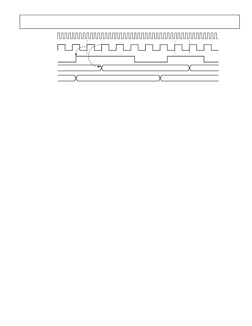
SYNC_CLK
SYSCLK
A
B
DATA 2
DATA 3
DATA 1
DATA IN
REGISTERS
DATA IN
I/O BUFFERS
DATA 1
DATA 2
DATA 3
I/O UPDATE
THE DEVICE REGISTERS AN I/O UPDATE AT POINT A. THE DATA IS TRANSFERRED FROM THE ASYNCHRONOUSLY LOADED I/O BUFFERS AT POINT B.
0
Figure 20. I/O Synchronization Timing Diagram
Synchronizing Multiple AD9859s
The AD9859 allows easy synchronization of multiple AD9859s.
There are three modes of synchronization available
to the user: an automatic synchronization mode, a software
controlled manual synchronization mode, and a hardware
controlled manual synchronization mode. In all cases, when a
user wants to synchronize two or more devices, the following
considerations must be observed. First, all units must share a
common clock source. Trace lengths and path impedance of the
clock tree must be designed to keep the phase delay of the dif-
ferent clock branches as closely matched as possible. Second, the
I/O UPDATE signal’s rising edge must be provided synchro-
nously to all devices in the system. Finally, regardless of the
internal synchronization method used, the DVDD_I/O supply
should be set to 3.3 V for all devices that are to be synchronized.
AVDD and DVDD should be left at 1.8 V.
In automatic synchronization mode, one device is chosen as a
master; the other device(s) is slaved to this master. When con-
figured in this mode, the slaves automatically synchronize their
internal clocks to the SYNC_CLK output signal of the master
device. To enter automatic synchronization mode, set the slave
device’s automatic synchronization bit (CFR1<23> = 1). Con-
nect the SYNC_IN input(s) to the master SYNC_CLK
output. The slave device continuously updates the phase rela-
tionship of its SYNC_CLK until it is in phase with the
SYNC_IN input, which is the SYNC_CLK of the master device.
When attempting to synchronize devices running at SYSCLK
speeds beyond 250 MSPS, the high speed sync enhancement
enable bit should be set (CFR2<11> = 1).
In software manual synchronization mode, the user forces the
device to advance the SYNC_CLK rising edge one SYSCLK
cycle (1/4 SYNC_CLK period). To activate the manual synchro-
nization mode, set the slave device’s software manual synchroni-
zation bit (CFR1<22> = 1). The bit (CFR1<22>) is cleared immedi-
ately. To advance the rising edge of the SYNC_CLK multiple times,
this bit needs to be set multiple times.
In hardware manual synchronization mode, the SYNC_IN
input pin is configured such that it advances the rising edge of
the SYNC_CLK signal each time the device detects a rising edge
on the SYNC_IN pin. To put the device into hardware manual
synchronization mode, set the hardware manual synchroniza-
tion bit (CFR2<10> = 1). Unlike the software manual synchro-
nization bit, this bit does not self-clear. Once the hardware
manual synchronization mode is enabled, all rising edges de-
tected on the SYNC_IN input cause the device to advance the
rising edge of the SYNC_CLK by one SYSCLK cycle until this
enable bit is cleared (CFR2<10> = 0).
Using a Single Crystal to Drive Multiple AD9859 Clock
Inputs
The AD9859 crystal oscillator output signal is available on the
CRYSTAL OUT pin, enabling one crystal to drive multiple
AD9859s. In order to drive multiple AD9859s with one crystal,
the CRYSTAL OUT pin of the AD9859 using the external crystal
should be connected to the REFCLK input of the other AD9859.
The CRYSTAL OUT pin is static until the CFR2<9> bit is set,
enabling the output. The drive strength of the CRYSTAL OUT
pin is typically very low, so this signal should be buffered prior
to using it to drive any loads.
SERIAL PORT OPERATION
With the AD9859, the instruction byte specifies read/write
operation and register address. Serial operations on the AD9859
occur only at the register level, not the byte level. For the
AD9859, the serial port controller recognizes the instruction
byte register address and automatically generates the proper
register byte address. In addition, the controller expects that all
bytes of that register will be accessed. It is a required that all
bytes of a register be accessed during serial I/O operations,
with one exception. The IOSYNC function can be used to
abort an I/O operation, thereby allowing less than all bytes
to be accessed.
相關PDF資料 |
PDF描述 |
|---|---|
| AD9859YSV | 400 MSPS, 10-Bit, 1.8 V CMOS Direct Digital Synthesizer |
| AD9859YSV-REEL7 | 400 MSPS, 10-Bit, 1.8 V CMOS Direct Digital Synthesizer |
| AD9862PCB | Mixed-Signal Front-End (MxFE⑩) Processor for Broadband Communications |
| AD9860 | Mixed-Signal Front-End (MxFE⑩) Processor for Broadband Communications |
| AD9860BST | Mixed-Signal Front-End (MxFE⑩) Processor for Broadband Communications |
相關代理商/技術參數 |
參數描述 |
|---|---|
| AD9859/PCB | 制造商:Analog Devices 功能描述:NCO, 400MSPS 10 BIT, 1.8V CMOS DIRECT DGTL SYNTHESIZER - Bulk |
| AD9859/PCBZ | 功能描述:BOARD EVAL FOR AD9859 RoHS:是 類別:編程器,開發系統 >> 評估演示板和套件 系列:AgileRF™ 標準包裝:1 系列:- 主要目的:電信,線路接口單元(LIU) 嵌入式:- 已用 IC / 零件:IDT82V2081 主要屬性:T1/J1/E1 LIU 次要屬性:- 已供物品:板,電源,線纜,CD 其它名稱:82EBV2081 |
| AD9859/PCBZ1 | 制造商:AD 制造商全稱:Analog Devices 功能描述:400 MSPS, 10-Bit,1.8 V CMOS Direct Digital Synthesizer |
| AD9859_09 | 制造商:AD 制造商全稱:Analog Devices 功能描述:400 MSPS, 10-Bit, 1.8 V CMOS Direct Digital Synthesizer |
| AD9859YSV | 制造商:Analog Devices 功能描述:Direct Digital Synthesizer 400MHz 1-DAC 10-Bit Serial 48-Pin TQFP EP 制造商:Analog Devices 功能描述:DDS 10BIT DAC 400MSPS SMD 9859 |
發布緊急采購,3分鐘左右您將得到回復。