- 您現在的位置:買賣IC網 > PDF目錄373969 > AD9860PCB (Analog Devices, Inc.) Mixed-Signal Front-End (MxFE⑩) Processor for Broadband Communications PDF資料下載
參數資料
| 型號: | AD9860PCB |
| 廠商: | Analog Devices, Inc. |
| 英文描述: | Mixed-Signal Front-End (MxFE⑩) Processor for Broadband Communications |
| 中文描述: | 混合寬帶通信信號前端(MxFE⑩)處理器 |
| 文件頁數: | 12/32頁 |
| 文件大小: | 617K |
| 代理商: | AD9860PCB |
第1頁第2頁第3頁第4頁第5頁第6頁第7頁第8頁第9頁第10頁第11頁當前第12頁第13頁第14頁第15頁第16頁第17頁第18頁第19頁第20頁第21頁第22頁第23頁第24頁第25頁第26頁第27頁第28頁第29頁第30頁第31頁第32頁
REV. 0
–12–
AD9860/AD9862
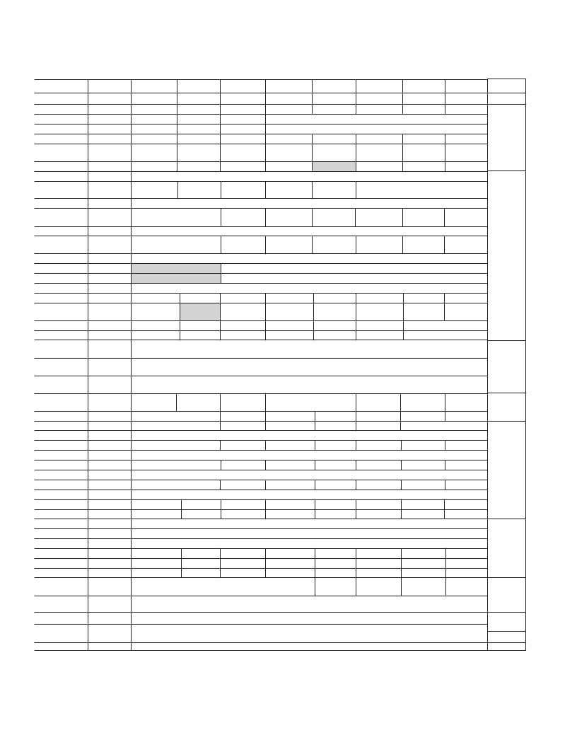
REGISTER MAP (0x00–0x3F)
1
Register Name
Address
2
Bit 7
Bit 6
Bit 5
Bit 4
Bit 3
Bit 2
Bit 1
Bit 0
General
Rx Power Down
Rx A
Rx B
Rx Misc
Rx I/F
0
1
2
3
4
5
SDIO BiDir
V
REF
(diff)
Byp Buffer A
Byp Buffer B
LSB First
V
REF
Soft Reset
Rx Digital
Rx Channel B
Rx Channel A Buffer B
Buffer A
All Rx
RxPGA A
RxPGA B
HS Duty Cycle
Shared Ref
Rx Retime
Twos
Complement
2 Channel
Keep
–
ve
Clk Duty
Mux Out
Three State
Inv RxSync
Rx Digital
RSV
Tx Power Down
6
7
8
Hilbert
Decimate
Reserved for Future Use
Alt Timing
Mode
Reserved for Future Use
TxOff Enable
Tx Digital
Tx Analog Power Down [2:0]
RSV
Tx A Offset
9
10
DAC A Offset [1:0]
DAC A Offset
Direction
Tx A Offset
Tx B Offset
11
12
DAC A Offset [9:2]
DAC B Offset [1:0]
DAC B Offset
Direction
Tx B Offset
Tx A Gain
Tx B Gain
Tx PGA Gain
Tx Misc
Tx I/F
13
14
15
16
17
18
DAC B Offset [9:2]
DAC A Coarse Gain
DAC B Coarse Gain
DAC A Fine Gain
DAC B Fine Gain
Tx PGA Gain
Slave Enable Tx PGA Fast
2 Edges
Tx Retime
Q/I Order
Inv TxSync
Twos
Complement
Keep
–
ve
Real Mix
Inverse
Sample
Hilbert
Neg. Coarse Tune
Coarse Modulation
Interleaved
Tx Digital
Tx Modulator
NCO Tuning
Word
NCO Tuning
Word
NCO Tuning
Word
DLL
19
20
2 Data Paths
Interpolation Control
Neg. Fine Tune
Fine Mode
21
FTW [7:0]
22
FTW [15:8]
23
FTW [23:16]
24
Reserved
Input Control ADC Div 2
Clock
DLL Multiplier
DLL
Power Down
DLL
FAST
Dis1
CLKOUT
Aux ADC A2
Aux ADC A2
Aux ADC A1
Aux ADC A1
Aux ADC B2
Aux ADC B2
Aux ADC B1
Aux ADC B1
Aux ADC Control
Aux ADC Clock
Aux DAC A
Aux DAC B
Aux DAC C
Aux DAC
Update Aux DAC 40
DAC Control
25
26
27
28
29
30
31
32
33
34
35
36
37
38
39
CLKOUT2 Divide Factor
Aux ADC A2 Data [1:0]
Inv2
Dis2
Inv1
Aux ADC A2 Data [9:2]
Aux ADC A1 Data [1:0]
Aux ADC A1 Data [9:2]
Aux ADC B2 Data [1:0]
Aux ADC B2 Data [9:2]
Aux ADC B1 Data [1:0]
Aux ADC B1 Data [9:2]
Select B
Aux SPI
SelBnot A
Refsel B
Start B
Refsel A
Select A
Start A
CLK/4
Aux DAC A
Aux DAC B
Aux DAC C
Slave Enable
Update C
Power Down C Power Down B Power Down A
Inv B
Update B
Update A
41
Inv C
Inv A
SigDelt
42
Sigma-Delta Control Word [3:0]
Flag
SigDelt
43
Sigma-Delta Control Word [11:4]
ADC Low Power
49, 50
Low Power Register for Rx Path Operation below 32 MSPS
RSV
44
–
62
Reserved for Future Use
63
Chip Rev ID
NOTES
1
When writing to a register with unassigned register bit(s), a logic low must be written to the unassigned bit(s). By default, after power up or RESET, all registers
are set low, except for the bits in the shaded boxes, which are set high.
2
Decimal
Purpose
SPI Setup
Receive
Path
Setup
Transmit
Path
Setup
NCO
Setup
Clock
Setup
Auxiliary
ADC Data
and Setup
Auxiliary
DAC Data
and Setup
Sigma-
Delta Data
and Setup
Rx Low
Power
Reserved
Chip ID
相關PDF資料 |
PDF描述 |
|---|---|
| AD9862 | Mixed-Signal Front-End (MxFE⑩) Processor for Broadband Communications |
| AD9862BST | Mixed-Signal Front-End (MxFE⑩) Processor for Broadband Communications |
| AD9864 | IF Digitizing Subsystem |
| AD9864-EB | IF Digitizing Subsystem |
| AD9864BCPZ | IF Digitizing Subsystem |
相關代理商/技術參數 |
參數描述 |
|---|---|
| AD9861 | 制造商:AD 制造商全稱:Analog Devices 功能描述:Mixed-Signal Front-End (MxFE⑩) Baseband Transceiver for Broadband Applications |
| AD9861-50EB | 制造商:Analog Devices 功能描述: |
| AD9861-50EBZ | 功能描述:BOARD EVALUATION FOR AD9861-50 RoHS:是 類別:RF/IF 和 RFID >> RF 評估和開發套件,板 系列:- 標準包裝:1 系列:- 類型:GPS 接收器 頻率:1575MHz 適用于相關產品:- 已供物品:模塊 其它名稱:SER3796 |
| AD9861-80EB | 制造商:Analog Devices 功能描述: |
| AD9861-80EBZ | 功能描述:BOARD EVALUATION FOR AD9861 RoHS:是 類別:RF/IF 和 RFID >> RF 評估和開發套件,板 系列:- 標準包裝:1 系列:- 類型:GPS 接收器 頻率:1575MHz 適用于相關產品:- 已供物品:模塊 其它名稱:SER3796 |
發布緊急采購,3分鐘左右您將得到回復。