- 您現在的位置:買賣IC網 > PDF目錄373969 > AD9860PCB (Analog Devices, Inc.) Mixed-Signal Front-End (MxFE⑩) Processor for Broadband Communications PDF資料下載
參數資料
| 型號: | AD9860PCB |
| 廠商: | Analog Devices, Inc. |
| 英文描述: | Mixed-Signal Front-End (MxFE⑩) Processor for Broadband Communications |
| 中文描述: | 混合寬帶通信信號前端(MxFE⑩)處理器 |
| 文件頁數: | 18/32頁 |
| 文件大小: | 617K |
| 代理商: | AD9860PCB |
第1頁第2頁第3頁第4頁第5頁第6頁第7頁第8頁第9頁第10頁第11頁第12頁第13頁第14頁第15頁第16頁第17頁當前第18頁第19頁第20頁第21頁第22頁第23頁第24頁第25頁第26頁第27頁第28頁第29頁第30頁第31頁第32頁
REV. 0
–18–
AD9860/AD9862
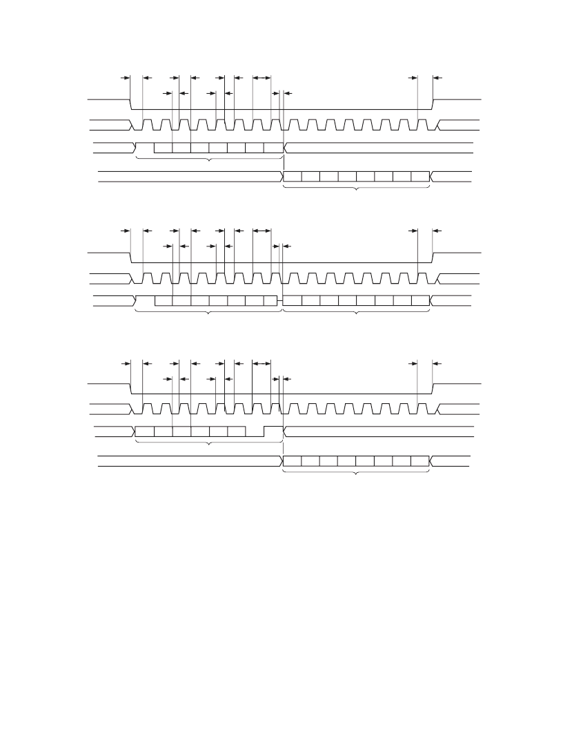
Read Operation
The read back of registers is a single data byte operation. The
readback can be configured to use three pins or four pins and can
be formatted as MSB first or LSB first. The instruction header
is written to the device either MSB or LSB first (depending on
the mode) followed by the 8-bit output data (appropriately MSB
or LSB justified). By default, the output data is sent to the dedicated
output pin (SDO). 3-wire operation can be configured by set-
ting the SDIO BiDir register. In 3-wire mode, the SDIO pin
will become an output pin after receiving the 8-bit instruction
header with a read back request.
Figure 2a shows an MSB first, 4-pin SPI read; Figure 2b shows an
MSB first, 3-pin read; and Figure 2c shows an LSB first, 4-pin read.
SYSTEM BLOCK DESCRIPTION
The AD9860/AD9862 integrates transmit and receive paths with
digital signal processing blocks and auxiliary features. The auxiliary
SDIO
SEN
SCLK
t
S
t
DS
t
DH
t
LO
t
HI
t
CLK
t
H
INSTRUCTION HEADER (REGISTER N)
SDO
SDIO
SEN
SCLK
SDIO
SEN
SCLK
SDO
t
DV
DON’T CARE
DON’T CARE
DON’T CARE
DON’T CARE
DON’T CARE
DON’T CARE
R/nW
2/n1
A5
A4
A3
A2
A1
A0
D7
D6
D5
D4
D3
D2
D1
D0
OUTPUT REGISTER DATA
t
S
t
DS
t
DH
t
LO
t
HI
t
CLK
t
DV
t
H
DON’T CARE
DON’T CARE
R/nW
2/n1
A5
A4
A3
A2
A1
A0
D7
D6
D5
D4
D3
D2
D1
D0
DON’T CARE
DON’T CARE
OUTPUT REGISTER DATA
INSTRUCTION HEADER
t
S
t
DS
t
DH
t
LO
t
HI
t
CLK
t
DV
t
H
DON’T CARE
R/nW
2/n1
DON’T CARE
DON’T CARE
DON’T CARE
DON’T CARE
DON’T CARE
A0
A1
A2
A3
A4
A5
D0
D1
D2
D3
D4
D5
D6
D7
OUTPUT REGISTER DATA
INSTRUCTION HEADER
Figure 2. SPI Read Examples a. (top) 4-Wire Interface, MSB first; b. (middle) 3-Wire Interface, MSB first;
c. (bottom) 4-Wire Interface, LSB first
features include two auxiliary ADCs, a programmable sigma-delta
output, three auxiliary DACs, integrated clock circuitry to generate
all internal clocks, and buffered output clocks from a single input
reference.
The AD9860/AD9862 system functionality is described in the
following four sections: the Transmit Block, Receive Block, Timing
Generation Block, and the Auxiliary Function Block. The following
sections provide a brief description of the blocks and applications
for the four sections.
TRANSMIT SECTION COMPONENTS
The transmit block (Tx) accepts and can process real or complex
data. The Tx interface is configurable for a variety of data formats
and has special processing options such as interpolation and Hilbert
filters. A detailed block diagram of the AD9860/AD9862 transmit
path is shown in Figure 3. The transmit block diagram is broken
into these stages: DAC (Block A), Coarse Modulation (Block B),
相關PDF資料 |
PDF描述 |
|---|---|
| AD9862 | Mixed-Signal Front-End (MxFE⑩) Processor for Broadband Communications |
| AD9862BST | Mixed-Signal Front-End (MxFE⑩) Processor for Broadband Communications |
| AD9864 | IF Digitizing Subsystem |
| AD9864-EB | IF Digitizing Subsystem |
| AD9864BCPZ | IF Digitizing Subsystem |
相關代理商/技術參數 |
參數描述 |
|---|---|
| AD9861 | 制造商:AD 制造商全稱:Analog Devices 功能描述:Mixed-Signal Front-End (MxFE⑩) Baseband Transceiver for Broadband Applications |
| AD9861-50EB | 制造商:Analog Devices 功能描述: |
| AD9861-50EBZ | 功能描述:BOARD EVALUATION FOR AD9861-50 RoHS:是 類別:RF/IF 和 RFID >> RF 評估和開發套件,板 系列:- 標準包裝:1 系列:- 類型:GPS 接收器 頻率:1575MHz 適用于相關產品:- 已供物品:模塊 其它名稱:SER3796 |
| AD9861-80EB | 制造商:Analog Devices 功能描述: |
| AD9861-80EBZ | 功能描述:BOARD EVALUATION FOR AD9861 RoHS:是 類別:RF/IF 和 RFID >> RF 評估和開發套件,板 系列:- 標準包裝:1 系列:- 類型:GPS 接收器 頻率:1575MHz 適用于相關產品:- 已供物品:模塊 其它名稱:SER3796 |
發布緊急采購,3分鐘左右您將得到回復。