- 您現在的位置:買賣IC網 > PDF目錄373969 > AD9860PCB (Analog Devices, Inc.) Mixed-Signal Front-End (MxFE⑩) Processor for Broadband Communications PDF資料下載
參數資料
| 型號: | AD9860PCB |
| 廠商: | Analog Devices, Inc. |
| 英文描述: | Mixed-Signal Front-End (MxFE⑩) Processor for Broadband Communications |
| 中文描述: | 混合寬帶通信信號前端(MxFE⑩)處理器 |
| 文件頁數: | 22/32頁 |
| 文件大小: | 617K |
| 代理商: | AD9860PCB |
第1頁第2頁第3頁第4頁第5頁第6頁第7頁第8頁第9頁第10頁第11頁第12頁第13頁第14頁第15頁第16頁第17頁第18頁第19頁第20頁第21頁當前第22頁第23頁第24頁第25頁第26頁第27頁第28頁第29頁第30頁第31頁第32頁
REV. 0
–22–
AD9860/AD9862
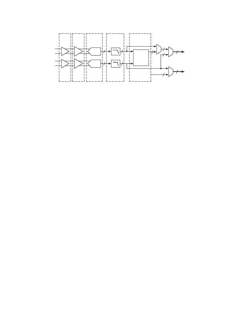
RECEIVE SECTION COMPONENTS
The receive block is configurable to process input signals of dif-
ferent formats and has special features such as an input buffer,
gain stage, and decimation filters. The AD9860/AD9862 receive
path block diagram is shown in Figure 6. The block diagram can
be broken into the following stages: Input Buffer (Block A),
RxPGA (Block B), dual, 10-/12-bit, 64 MSPS ADC (Block C),
Decimation filter (Block D), Digital Hilbert Block (Block E),
and a Data Output Multiplexer. The function of each stage is
explained in the following paragraphs.
Input Buffer Stage
The input buffer stage buffers the input signal on-chip for both
receive paths. The buffer stage has two main benefits, providing
a constant input impedance and reducing any
“
kick-back
”
noise
that might be generated on-chip, affecting the analog input signal.
The Rx path sampling mode can be split into two categories,
depending on the frequency of the input signal. When sampling
input signals up to Nyquist of the ADC, the sampling is referred to
as Nyquist sampling. When sampling at rates above ADC Nyquist
rate, the sampling is referred to as IF sampling or undersampling.
For Nyquist sampling, the input buffer provides a constant 200
W
impedance over the entire input signal range. The constant input
impedance accommodates matching networks to ensure proper
transfer of signal to the input of the device. The input buffer is
self-biased to ~ 2 V, and therefore the input signal should be
ac-coupled to the Rx differential input or have a common-mode
voltage of about 2 V. If an external buffer is present, the internal
input buffer can be bypassed and powered down to reduce power
consumption. The input buffer accepts up to a 2 V p-p input
signal for maximum SNR performance. Optimal THD perfor-
mance occurs with 1 V p-p input signal.
For IF sampling, the input buffer can be used with input signals
up to about 100 MHz, the 3 dB bandwidth of the buffer. When
undersampling the input signal, the output spectrum will contain
an aliased version of the original, higher frequency signal. As was
the case with Nyquist sampling, the input signal should be
ac-coupled to the Rx differential input or have a common-mode
voltage of ~ 2 V. For input signals over 100 MHz to about 250 MHz,
the input buffer needs to be bypassed and an external input
buffer is required. In the case that the input buffer is bypassed,
the input circuit is a switched capacitor network. The switching
input impedance during the sample phase is about 1/(2( )FC),
where F is the input frequency and C is the input capacitance
(about 4 pF). During hold mode, the input impedance is > 1 M
W
.
RxPGA
The RxPGA stage has a Programmable Gain Amplifier that can be
used to amplify the input signal to utilize the entire input range
of the ADC. The RxPGA stage provides a 0 dB to 20 dB gain
range in steps of about 1 dB. The Rx channel independent gain
control is accomplished through two 5-bit SPI programmable
RxPGA A/B registers. The gain curve is linear in dB with a minimum
gain setting (0 dB, nominally) of hex00 and a maximum gain
setting (20 dB, nominally) of hex14.
The RxPGA stage can provide up to a 2 V p-p signal to the
ADC input.
Analog-to-Digital (A/D) Converter
The analog-to-digital converter (ADC) stage consists of two
high performance 10-/12-bit, 64 MSPS analog-to-digital (A/D)
converters. The dual A/D converter paths are fully independent,
except for a shared internal bandgap reference source, V
REF
. Each
of the A/D converter
’
s paths consists of a front-end sample and
hold amplifier followed by a pipelined, switched capacitor, A/D
converter. The pipelined A/D converter is divided into three sections,
consisting of a 4-bit first stage followed by eight 1.5-bit stages and
a final 3-bit flash. Each stage provides sufficient overlap to correct
for flash errors in the preceding stages. The quantized outputs
from each stage are combined into a final 12-bit result through
a digital correction logic block. The pipelined architecture permits
the first stage to operate on a new input sample while the remain-
ing stages operate on preceding samples. Sampling occurs on the
rising clock edge.
Each stage of the pipeline, excluding the last, consists of a low
resolution flash A/D connected to a switched capacitor DAC and
interstage residue amplifier (MDAC). The residue amplifier magni-
fies the difference between the reconstructed DAC output and the
flash input for the next stage in the pipeline. One bit of redundancy
is used in each one of the stages to facilitate digital correction of
flash errors. The last stage simply consists of a flash A/D.
A stable and accurate 1.0 V bandgap voltage reference is built into
the AD9860/AD9862 and is used to set a 2 V p-p differential input
range. The internally generated reference should be decoupled
at the V
REF
pin using a 10
m
F and a 0.1
m
F capacitor in parallel
to ground. Separate top and bottom references, V
RT
and V
RB
,
for each converter are generated from V
REF
and should also be
decoupled. Recommended decoupling for the top and bottom
references consists of using 10
m
F and 0.1
m
F capacitors in parallel
between the differential reference pins, and a 0.1
m
F capacitor
ADC
LOW-PASS
DECIMATION
FILTER
PGA
1
VIN+A
VIN–A
ADC
PGA
1
VIN+B
VIN–B
HILBERT
FILTER
BLOCK A BLOCK B
BLOCK C
BLOCK D
BLOCK E
RxA DATA
[0:11]
RxB DATA
[0:11]
Figure 6. Receive Section Block Diagram
相關PDF資料 |
PDF描述 |
|---|---|
| AD9862 | Mixed-Signal Front-End (MxFE⑩) Processor for Broadband Communications |
| AD9862BST | Mixed-Signal Front-End (MxFE⑩) Processor for Broadband Communications |
| AD9864 | IF Digitizing Subsystem |
| AD9864-EB | IF Digitizing Subsystem |
| AD9864BCPZ | IF Digitizing Subsystem |
相關代理商/技術參數 |
參數描述 |
|---|---|
| AD9861 | 制造商:AD 制造商全稱:Analog Devices 功能描述:Mixed-Signal Front-End (MxFE⑩) Baseband Transceiver for Broadband Applications |
| AD9861-50EB | 制造商:Analog Devices 功能描述: |
| AD9861-50EBZ | 功能描述:BOARD EVALUATION FOR AD9861-50 RoHS:是 類別:RF/IF 和 RFID >> RF 評估和開發套件,板 系列:- 標準包裝:1 系列:- 類型:GPS 接收器 頻率:1575MHz 適用于相關產品:- 已供物品:模塊 其它名稱:SER3796 |
| AD9861-80EB | 制造商:Analog Devices 功能描述: |
| AD9861-80EBZ | 功能描述:BOARD EVALUATION FOR AD9861 RoHS:是 類別:RF/IF 和 RFID >> RF 評估和開發套件,板 系列:- 標準包裝:1 系列:- 類型:GPS 接收器 頻率:1575MHz 適用于相關產品:- 已供物品:模塊 其它名稱:SER3796 |
發布緊急采購,3分鐘左右您將得到回復。