- 您現在的位置:買賣IC網 > PDF目錄373969 > AD9874BST (ANALOG DEVICES INC) IF Digitizing Subsystem PDF資料下載
參數資料
| 型號: | AD9874BST |
| 廠商: | ANALOG DEVICES INC |
| 元件分類: | 通信及網絡 |
| 英文描述: | IF Digitizing Subsystem |
| 中文描述: | SPECIALTY TELECOM CIRCUIT, PQFP48 |
| 封裝: | PLASTIC, MS-026BBC, LQFP-48 |
| 文件頁數: | 18/40頁 |
| 文件大小: | 744K |
| 代理商: | AD9874BST |
第1頁第2頁第3頁第4頁第5頁第6頁第7頁第8頁第9頁第10頁第11頁第12頁第13頁第14頁第15頁第16頁第17頁當前第18頁第19頁第20頁第21頁第22頁第23頁第24頁第25頁第26頁第27頁第28頁第29頁第30頁第31頁第32頁第33頁第34頁第35頁第36頁第37頁第38頁第39頁第40頁
REV. 0
–18–
AD9874
AD9874
CLKOUT
RSCLK
RFS
DR
PC
PE
PD
SCK
SEL
MOSI
MISO
DOUTB
FS
DOUTA
SPI
SSI
ADSP-2153X
SERIAL
PORT
SPI-PORT
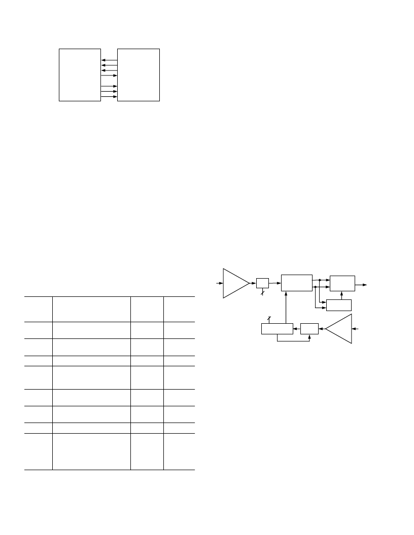
Figure 4b. Example of AD9874 and ADSP-2153x Interface
As shown in Figure 4b, AD9874’s synchronous serial interface
(SSI) links the receive data stream to the DSP’s Serial Port (SPORT).
For AD9874 set-up and register programming, the device connects
directly to ADSP-2153x’s SPI-PORT. Dedicated select lines (SEL)
allow the ADSP-2153x to program and read back registers of
multiple devices using only one SPI port. The DSP driver code
(http://products.analog.com/products/info.aspproduct=AD9874
).
POWER CONTROL
To allow power consumption to be minimized, the AD9874
possesses numerous SPI-programmable power-down and bias
control bits. The AD9874 powers up with all of its functional
blocks placed into a standby state (i.e., STBY Register default is
0xFF). Each major block may then be powered up by writing a 0
to the appropriate bit of the STBY Register. This scheme provides
the greatest flexibility for configuring the IC to a specific appli-
cation as well as for tailoring the IC’s power-down and wake-up
characteristics. Table VI summarizes the function of each of the
STBY bits. Note, when all the blocks are in standby, the master
reference circuit is also put into standby and thus the current is
reduced by a further 0.4 mA.
Table VI. Standby Control Bits
Current
Reduction Wake-Up
(mA)
1
STBY
Bit
Effect
Time (ms)
7:REF
Voltage Reference OFF;
all biasing shut down.
0.6
<0.1 (C
REF
= 4.7 nF)
6:LO
LO Synthesizer OFF,
IOUTL three-state.
1.2
Note 2
5:CKO
Clock Oscillator OFF
1.1
Note 2
4:CK
Clock Synthesizer OFF,
IOUTC three-state. Clock
buffer OFF if ADC is OFF.
1.3
Note 2
3:GC
Gain Control DAC OFF.
GCP and GCN three-state.
0.2
Depends
on C
GC
2:LNAMX LNA and Mixer OFF. CXVM,
CXVL, and CXIF three-state.
8.2
<2.2
1:Unused
0:ADC
ADC OFF; Clock Buffer
OFF
if CLK synthesizer OFF;
VCM
three-state; Clock to the digital
filter halted; Digital outputs
static.
9.2
<0.1
NOTES
1
When all blocks are in standby, the master reference circuit is also put into
standby and thus the current is reduced by a further 0.4 mA.
2
Wake-up time is dependent on programming and/or external components.
The AD9874 also allows control over the bias current in the LNA,
mixer, and clock oscillator. The effects on current consumption
and system performance are described in the section dealing
with the affected block.
LO Synthesizer
The LO Synthesizer shown in Figure 5 is a fully programmable
PLL capable of 6.25 kHz resolution at input frequencies up to
300 MHz and reference clocks of up to 25 MHz. It consists of a
low noise digital phase-frequency detector (PFD), a variable
output current charge pump (CP), a 14-bit reference divider,
programmable A and B counters, and a dual-modulus 8/9 prescaler.
The A (3-bit) and B (13-bit) counters, in conjunction with the
dual 8/9 modulus prescaler, implement an N divider with N =
8 B + A. In addition, the 14-bit reference counter (R Counter)
allows selectable input reference frequencies, f
REF
,
at the PFD
input. A complete PLL (phase-locked loop) can be implemented
if the synthesizer is used with an external loop filter and VCO
(voltage controlled oscillator).
The A, B, and R counters can be programmed via the following
registers: LOA, LOB, and LOR. The charge pump output current
is programmable via the LOI Register from 0.625 mA to 5.0 mA
using the following equation:
IPUMP
An on-chip fast acquire function (enabled by the LOF bit)
automatically increases the output current for faster settling
during channel changes. The synthesizer may also be disabled
using the LO standby bit located in the STBY Register.
LOI
mA
=
+
×
(
)
.
1
0 625
(2)
FAST
ACQUIRE
8/9
A, B
COUNTERS
LO
BUFFER
LOA, LOB
f
FROM
VCO
REF
BUFFER
f
REF
LOR
R
F
REF
PHASE/
FREQUENCY
DETECTOR
TO EXTERNAL
LOOP
FILTER
F
LO
CHARGE
PUMP
Figure 5. LO Synthesizer
The LO (and CLK) synthesizer works in the following manner.
The externally supplied reference frequency, f
REF
, is buffered and
divided by the value held in the R counter. The internal f
REF
is
then compared to a divided version of the VCO frequency,
f
LO
.
The phase/frequency detector provides UP and DOWN pulses
whose widths vary depending upon the difference in phase and
frequency of its two input signals. The UP/DOWN pulses con-
trol the charge pump making current available to charge the
external low-pass loop filter when there is a discrepancy between
the inputs of the PFD. The output of the low-pass filter feeds an
external VCO whose output frequency,
f
LO
, is driven such that
its divided down version,
f
LO
,
matches that of f
REF
,
thus closing
the feedback loop.
The synthesized frequency is related to the reference frequency
and the LO Register contents as follows:
f
LOB
LOA
LOR
LO
(
)/
8
Note, the minimum allowable value in the
LOB
Register is 3 and
its value must always be greater than that loaded into
LOA
.
f
REF
=
×
+
×
(3)
相關PDF資料 |
PDF描述 |
|---|---|
| AD9874EB | IF Digitizing Subsystem |
| AD9875BSTRL | Broadband Modem Mixed-Signal Front End |
| AD9875 | Broadband Modem Mixed-Signal Front End |
| AD9875-EB | Broadband Modem Mixed-Signal Front End |
| AD9875BST | Broadband Modem Mixed-Signal Front End |
相關代理商/技術參數 |
參數描述 |
|---|---|
| AD9874EB | 制造商:AD 制造商全稱:Analog Devices 功能描述:IF Digitizing Subsystem |
| AD9874-EB | 制造商:Analog Devices 功能描述: |
| AD9874-EBZ | 功能描述:BOARD EVAL FOR AD9874 制造商:analog devices inc. 系列:- 零件狀態:有效 類型:數字轉換器 頻率:10MHz ~ 300MHz 配套使用產品/相關產品:AD9874 所含物品:板 標準包裝:1 |
| AD9875 | 制造商:AD 制造商全稱:Analog Devices 功能描述:Broadband Modem Mixed-Signal Front End |
| AD9875BST | 制造商:Analog Devices 功能描述:Modem Chip Single 48-Pin LQFP 制造商:Rochester Electronics LLC 功能描述:10B BROADBAND MODEM MXFE CONVERTER - Tape and Reel |
發布緊急采購,3分鐘左右您將得到回復。