- 您現在的位置:買賣IC網 > PDF目錄373970 > AD9877-EB (Analog Devices, Inc.) Mixed-Signal Front End Set-Top Box, Cable Modem PDF資料下載
參數資料
| 型號: | AD9877-EB |
| 廠商: | Analog Devices, Inc. |
| 英文描述: | Mixed-Signal Front End Set-Top Box, Cable Modem |
| 中文描述: | 混合信號前端機頂盒,電纜調制解調器 |
| 文件頁數: | 22/36頁 |
| 文件大小: | 1094K |
| 代理商: | AD9877-EB |
第1頁第2頁第3頁第4頁第5頁第6頁第7頁第8頁第9頁第10頁第11頁第12頁第13頁第14頁第15頁第16頁第17頁第18頁第19頁第20頁第21頁當前第22頁第23頁第24頁第25頁第26頁第27頁第28頁第29頁第30頁第31頁第32頁第33頁第34頁第35頁第36頁
AD9877
SERIAL INTERFACE FOR REGISTER CONTROL
The AD9877 serial port is a flexible, synchronous serial
communication port allowing easy interface to many industry-
standard microcontrollers and microprocessors. The interface
allows read/write access to all registers that configure the
AD9877. Single or multiple byte transfers are supported. Also,
the interface can be programmed to read words either MSB first
or LSB first. The serial interface port I/O of the AD9877 can be
configured to have one bidirectional I/O (SDIO) pin or two
unidirectional I/O (SDIO/SDO) pins.
Rev. B | Page 22 of 36
GENERAL OPERATION OF THE SERIAL INTERFACE
There are two phases to a communication cycle with the
AD9877. Phase 1 is the instruction cycle, which is the writing of
an instruction byte into the AD9877 that is coincident with the
first eight SCLK rising edges. The instruction byte provides the
AD9877 serial port controller with information regarding the
data transfer cycle, Phase 2 of the communication cycle. The
Phase 1 instruction byte defines whether the upcoming data
transfer is a read or write, the number of bytes in the data
transfer, and the starting register address for the first byte of the
data transfer. The first eight SCLK rising edges of each
communication cycle are used to write the instruction byte into
the AD9877.
The eight remaining SCLK edges are for Phase 2 of the
communication cycle. Phase 2 is the actual data transfer
between the AD9877 and the system controller. Phase 2 of the
communication cycle is a transfer of 1 to 4 data bytes as
determined by the instruction byte. Registers change
immediately upon writing to the last bit of each transfer byte.
INSTRUCTION BYTE
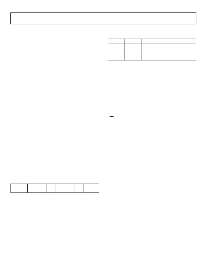
Table 9 illustrates the information contained in the instruction byte.
Table 9. Instruction Byte Information
MSB
I7
I6
I5
I4
R/W
N1
N0
A4
I3
A3
I2
A2
I1
A1
LSB
I0
A0
The R/W bit of the instruction byte determines whether a read
or a write data transfer will occur after the instruction byte
write. Logic high indicates a read operation. Logic low indicates
a write operation. The N1:N0 bits determine the number of
bytes to be transferred during the data transfer cycle. The bit
decodes are shown in Table 10.
Table 10. Bit Decodes
N1
0
0
1
1
N0
0
1
0
1
Description
Transfer 1 byte
Transfer 2 bytes
Transfer 3 bytes
Transfer 4 bytes
The Bits A4:A0 determine which register is accessed during the
data transfer portion of the communication cycle. For multibyte
transfers, this address is the starting byte address. The
remaining register addresses are generated by the AD9877.
SERIAL INTERFACE PORT PIN DESCRIPTION
SCLK—Serial Clock
The serial clock pin is used to synchronize data transfers from
the AD9877 and to run the serial port state machine. The
maximum SCLK frequency is 15 MHz. Input data to the
AD9877 is sampled upon the rising edge of SCLK. Output data
changes upon the falling edge of SCLK.
CS—Chip Select
Active low input starts and gates a communication cycle. It
allows multiple devices to share a common serial port bus. The
SDO and SDIO pins go to a high impedance state when CS is
high. Chip select should stay low during the entire
communication cycle.
SDIO—Serial Data I/O
Data is always written into the AD9877 on this pin. However,
this pin can be used as a bidirectional data line. The configuration
of this pin is controlled by Bit 7 of Register 0x00. The default is
Logic 0, which configures the SDIO pin as unidirectional.
SDO—Serial Data Out
Data is read from this pin for protocols that use separate lines
for transmitting and receiving data. When the AD9877 operates
in a single bidirectional I/O mode, this pin does not output data
and is set to a high impedance state.
MSB/LSB TRANSFERS
The AD9877 serial port can support both the MSB-first or the
least significant bit LSB-first data formats. This functionality is
controlled by the LSB-first bit in Register 0x00. The default is
MSB first.
When this bit is set active high, the AD9877 serial port is in
LSB-first format. In LSB-first mode, the instruction byte and
data bytes must be written from the LSB to the MSB. In LSB-
first mode, the serial port internal byte address generator
increments for each byte of the multibyte communication cycle.
相關PDF資料 |
PDF描述 |
|---|---|
| AD9882KST-100 | Dual Interface for Flat Panel Displays |
| AD9882KST-140 | Dual Interface for Flat Panel Displays |
| AD9882 | Dual Interface for Flat Panel Displays |
| AD9883ABST-RL140 | 110 MSPS/140 MSPS Analog Interface for Flat Panel Displays |
| AD9883AKST-110 | 110 MSPS/140 MSPS Analog Interface for Flat Panel Displays |
相關代理商/技術參數 |
參數描述 |
|---|---|
| AD9878 | 制造商:AD 制造商全稱:Analog Devices 功能描述:Mixed-Signal Front End for Broadband Applications |
| AD9878BST | 制造商:Analog Devices 功能描述:Mixed Signal Front End 100-Pin LQFP |
| AD9878BSTRL | 制造商:Analog Devices 功能描述:Mixed Signal Front End 100-Pin LQFP T/R 制造商:Analog Devices 功能描述:MIXED SGNL FRONT END 100LQFP - Tape and Reel |
| AD9878BSTZ | 功能描述:IC FRONT-END MIXED-SGNL 100-LQFP RoHS:是 類別:集成電路 (IC) >> 數據采集 - 模擬前端 (AFE) 系列:- 產品培訓模塊:Lead (SnPb) Finish for COTS Obsolescence Mitigation Program 標準包裝:2,500 系列:- 位數:- 通道數:2 功率(瓦特):- 電壓 - 電源,模擬:3 V ~ 3.6 V 電壓 - 電源,數字:3 V ~ 3.6 V 封裝/外殼:32-VFQFN 裸露焊盤 供應商設備封裝:32-QFN(5x5) 包裝:帶卷 (TR) |
| AD9878-EB | 制造商:Analog Devices 功能描述:EVAL KIT FOR MIXED-SGNL FRONT END FOR BROADBAND APPLICATIONS - Bulk |
發布緊急采購,3分鐘左右您將得到回復。