- 您現在的位置:買賣IC網 > PDF目錄373970 > AD9877-EB (Analog Devices, Inc.) Mixed-Signal Front End Set-Top Box, Cable Modem PDF資料下載
參數資料
| 型號: | AD9877-EB |
| 廠商: | Analog Devices, Inc. |
| 英文描述: | Mixed-Signal Front End Set-Top Box, Cable Modem |
| 中文描述: | 混合信號前端機頂盒,電纜調制解調器 |
| 文件頁數: | 30/36頁 |
| 文件大小: | 1094K |
| 代理商: | AD9877-EB |
第1頁第2頁第3頁第4頁第5頁第6頁第7頁第8頁第9頁第10頁第11頁第12頁第13頁第14頁第15頁第16頁第17頁第18頁第19頁第20頁第21頁第22頁第23頁第24頁第25頁第26頁第27頁第28頁第29頁當前第30頁第31頁第32頁第33頁第34頁第35頁第36頁
AD9877
RECEIVE PATH (Rx)
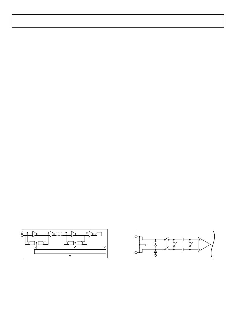
ADC THEORY OF OPERATION
The analog-to-digital converters of the AD9877 implement
pipelined multistage architectures to achieve high sample rates
while consuming low power. Each ADC distributes the
conversion over several smaller ADC subblocks, refining the
conversion with progressively higher accuracy as it passes the
results from stage to stage.
Rev. B | Page 30 of 36
As a consequence of the distributed conversion, ADCs require a
small fraction of the 2
n
comparators used in a traditional n-bit
flash-type ADC. A sample-and-hold function within each of the
stages permits the first stage to operate on a new input sample
while the remaining stages operate on preceding samples. Each
stage of the pipeline, excluding the last, consists of a low
resolution flash ADC connected to a switched capacitor DAC
and interstage residue amplifier (MDAC). The residue amplifier
amplifies the difference between the reconstructed DAC output
and the flash input for the next stage in the pipeline. One bit of
redundancy is used in each stage to facilitate digital correction
of flash errors. The last stage simply consists of a flash ADC.
The analog inputs of the AD9877 incorporate a novel structure
that merges the input sample-and-hold amplifiers (SHA) and
the first pipeline residue amplifiers into single, compact
switched capacitor circuits. This structure achieves considerable
noise and power savings over a conventional implementation
that uses separate amplifiers by eliminating one amplifier in the
pipeline. By matching the sampling network of the input SHA
with the first stage flash ADC, the ADCs can sample inputs well
beyond the Nyquist frequency with no degradation in
performance.
The digital data outputs of the ADCs are represented in straight
binary format. They saturate to full scale or zero scale when the
input signal exceeds the input voltage range.
RECEIVE TIMING
The AD9877 sends multiplexed data to the RxIQ outputs upon
every rising edge of MCLK. The data stream consists of two
nibbles of I data followed by two nibbles of Q data. The
RxSYNC pulse frames the I/Q data and is coincidentally high
with the most significant nibble of the I data-word. If the 8-bit
I/Q ADC is in power-down mode, the RxSYNC signal will not
be generated.
The 12-bit ADC data is sent to the IF[11:0] outputs upon every
second falling edge of MCLK.
In its default setting, the REFCLK pin provides a buffered
version of f
OSCIN
. REFCLK can be used as a qualifying clock for
the Rx data when the ratio between the OSCIN multiplier and
the OSCIN divider is programmed to be 2 (M/N = 2) or when
the ADC sampling is selected to be derived from f
OSCIN
directly.
DRIVING THE ANALOG INPUTS
Figure 40 illustrates the equivalent analog inputs of the AD9877
(a switched capacitor input). Bringing CLK to a logic high
opens Switch S3 and closes Switches S1 and S2. The input
source is connected to AIN and must charge capacitor C
H
during this time. Bringing CLK to a logic low opens switch S2,
and then Switch S1 opens followed by closing switch S3. This
places the input into hold mode.
The structure of the input SHA places certain requirements on
the input drive source. The combination of the pin capacitance
and the hold capacitance of C
H
is typically less than 5 pF. The
input source must be able to charge or discharge this
capacitance to its n-bit accuracy in one-half of a clock cycle.
When the SHA goes into track mode, the input source must
charge or discharge capacitor C
H
from the voltage already stored
on C
H
to the new voltage. In the worst case, a full-scale voltage
step on the input source must provide the charging current
through the R
ON
(100 Ω) of Switch S1 and quickly (within
1/2 CLK period) settle. This situation corresponds to driving a
low input impedance.
D/A
A/D
A/D
SHA
CORRECTION LOGIC
D/A
A/D
SHA
GAIN
AINP
AINN
AD9877
0
Figure 39. ADC Architecture
AINP
AINN
2k
Ω
2k
Ω
V
BIAS
S1
S3
C
P
C
P
C
H
C
H
S2
AD9877
0
Figure 40. Differential Input Architecture
相關PDF資料 |
PDF描述 |
|---|---|
| AD9882KST-100 | Dual Interface for Flat Panel Displays |
| AD9882KST-140 | Dual Interface for Flat Panel Displays |
| AD9882 | Dual Interface for Flat Panel Displays |
| AD9883ABST-RL140 | 110 MSPS/140 MSPS Analog Interface for Flat Panel Displays |
| AD9883AKST-110 | 110 MSPS/140 MSPS Analog Interface for Flat Panel Displays |
相關代理商/技術參數 |
參數描述 |
|---|---|
| AD9878 | 制造商:AD 制造商全稱:Analog Devices 功能描述:Mixed-Signal Front End for Broadband Applications |
| AD9878BST | 制造商:Analog Devices 功能描述:Mixed Signal Front End 100-Pin LQFP |
| AD9878BSTRL | 制造商:Analog Devices 功能描述:Mixed Signal Front End 100-Pin LQFP T/R 制造商:Analog Devices 功能描述:MIXED SGNL FRONT END 100LQFP - Tape and Reel |
| AD9878BSTZ | 功能描述:IC FRONT-END MIXED-SGNL 100-LQFP RoHS:是 類別:集成電路 (IC) >> 數據采集 - 模擬前端 (AFE) 系列:- 產品培訓模塊:Lead (SnPb) Finish for COTS Obsolescence Mitigation Program 標準包裝:2,500 系列:- 位數:- 通道數:2 功率(瓦特):- 電壓 - 電源,模擬:3 V ~ 3.6 V 電壓 - 電源,數字:3 V ~ 3.6 V 封裝/外殼:32-VFQFN 裸露焊盤 供應商設備封裝:32-QFN(5x5) 包裝:帶卷 (TR) |
| AD9878-EB | 制造商:Analog Devices 功能描述:EVAL KIT FOR MIXED-SGNL FRONT END FOR BROADBAND APPLICATIONS - Bulk |
發布緊急采購,3分鐘左右您將得到回復。