- 您現在的位置:買賣IC網 > PDF目錄373973 > AD9995KCPRL (ANALOG DEVICES INC) 12-Bit CCD Signal Processor with Precision Timing ⑩ Generator PDF資料下載
參數資料
| 型號: | AD9995KCPRL |
| 廠商: | ANALOG DEVICES INC |
| 元件分類: | 消費家電 |
| 英文描述: | 12-Bit CCD Signal Processor with Precision Timing ⑩ Generator |
| 中文描述: | SPECIALTY CONSUMER CIRCUIT, QCC56 |
| 封裝: | 8 X 8 MM, MO-220-VLLD-2, LFCSP-56 |
| 文件頁數: | 30/60頁 |
| 文件大小: | 1593K |
| 代理商: | AD9995KCPRL |
第1頁第2頁第3頁第4頁第5頁第6頁第7頁第8頁第9頁第10頁第11頁第12頁第13頁第14頁第15頁第16頁第17頁第18頁第19頁第20頁第21頁第22頁第23頁第24頁第25頁第26頁第27頁第28頁第29頁當前第30頁第31頁第32頁第33頁第34頁第35頁第36頁第37頁第38頁第39頁第40頁第41頁第42頁第43頁第44頁第45頁第46頁第47頁第48頁第49頁第50頁第51頁第52頁第53頁第54頁第55頁第56頁第57頁第58頁第59頁第60頁
AD9995
–30–
DRAFT IMAGE
SERIAL
WRITES
VD
VSG
SUBCK
STROBE
MSHUT
MECHANICAL
SHUTTER
VSUB
CCD
OUT
1
9
10
8
7
6
2
t
EXP
4
5
3
OPEN
CLOSED
MODE 0
MODE 1
10
10
10
OPEN
STILL IMAGE 3RD FIELD
STILL IMAGE 2ND FIELD
STILL IMAGE 1ST FIELD
DRAFT IMAGE
DRAFT IMAGE
STILL IMAGE READOUT
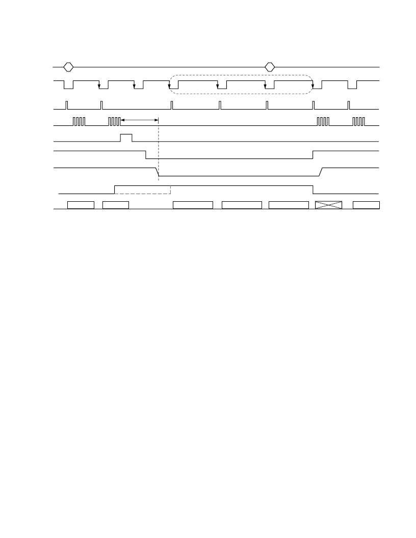
Figure 32. Example of Exposure and Still Image Readout Using Shutter Signals and Mode Register
1. Write to the READOUT register (Addr. 0x61) to specify
the number of fields to further suppress SUBCK while the
CCD data is read out. In this example, READOUT = 3.
Write to the EXPOSURE register (Addr. 0x62) to specify
the number of fields to suppress SUBCK and VSG outputs
during exposure. In this example, EXPOSURE = 1.
Write to the TRIGGER register (Addr. 0x60) to enable the
STROBE, MSHUT, and VSUB signals, and to start the
exposure/readout operation. To trigger all of these events (as
in Figure 32), set the register TRIGGER = 31. Readout will
automatically occur after the exposure period is finished.
Write to the MODE register (Addr. 0x1B) to configure the
next five fields. The first two fields during exposure are the
same as the current draft mode fields, and the following
three fields are the still frame readout fields. The registers
for the Draft mode field and the three readout fields have
already been programmed.
2. VD/HD falling edge will update the serial writes from 1.
3. If VSUB mode = 0 (Addr. 0x67), VSUB output turns on at
the line specified in the VSUBON register (Addr. 0x68).
4. STROBE output turns on and off at the location specified
in the STROBEON and OFF registers (Addr. 0x6E to
Addr. 0x71).
5. MSHUT output turns off at the location specified in the
MSHUTOFF registers (Addr. 0x6B and 0x6C).
6. The next VD falling edge will automatically start the first
readout field.
7. The next VD falling edge will automatically start the second
readout field.
8. The next VD falling edge will automatically start the third
readout field.
9. Write to the MODE register to reconfigure the single Draft
mode field timing.
Write to the MSHUTON register (Addr. 0x6A) to open the
mechanical shutter.
10. VD/HD falling edge will update the serial write from 9.
VSG outputs return to Draft mode timing.
SUBCK output resumes operation.
MSHUT output returns to the on position (active or open).
VSUB output returns to the off position (inactive).
EXPOSURE AND READOUT EXAMPLE
REV. 0
相關PDF資料 |
PDF描述 |
|---|---|
| AD9995 | 12-Bit CCD Signal Processor with Precision Timing ⑩ Generator |
| ADA4000-2ARMZ-RL | Low Cost, Precision JFET Input Operational Amplifiers |
| ADA4000-1 | Low Cost, Precision JFET Input Operational Amplifiers |
| ADA4000-1_07 | Low Cost, Precision JFET Input Operational Amplifiers |
| ADA4000-1ARZ | Low Cost, Precision JFET Input Operational Amplifiers |
相關代理商/技術參數 |
參數描述 |
|---|---|
| AD9995KCPZ | 功能描述:IC CCD SIGNAL PROCESSOR 56-LFCSP RoHS:是 類別:集成電路 (IC) >> 接口 - 傳感器和探測器接口 系列:- 其它有關文件:Automotive Product Guide 產品培訓模塊:Lead (SnPb) Finish for COTS Obsolescence Mitigation Program 標準包裝:74 系列:- 類型:觸控式傳感器 輸入類型:數字 輸出類型:數字 接口:JTAG,串行 電流 - 電源:100µA 安裝類型:表面貼裝 封裝/外殼:20-TSSOP(0.173",4.40mm 寬) 供應商設備封裝:20-TSSOP 包裝:管件 |
| AD9995KCPZRL | 功能描述:IC CCD SIGNAL PROCESSOR 56-LFCSP RoHS:是 類別:集成電路 (IC) >> 接口 - 傳感器和探測器接口 系列:- 其它有關文件:Automotive Product Guide 產品培訓模塊:Lead (SnPb) Finish for COTS Obsolescence Mitigation Program 標準包裝:74 系列:- 類型:觸控式傳感器 輸入類型:數字 輸出類型:數字 接口:JTAG,串行 電流 - 電源:100µA 安裝類型:表面貼裝 封裝/外殼:20-TSSOP(0.173",4.40mm 寬) 供應商設備封裝:20-TSSOP 包裝:管件 |
| AD9995KCPZRL7 | 制造商:Rochester Electronics LLC 功能描述: 制造商:Analog Devices 功能描述: |
| AD9996BBCZ | 制造商:Rochester Electronics LLC 功能描述:14B 40 MSPS AFETG CONVERTER - Bulk |
| AD9996BBCZRL | 制造商:Rochester Electronics LLC 功能描述:- Bulk |
發布緊急采購,3分鐘左右您將得到回復。