- 您現在的位置:買賣IC網 > PDF目錄373973 > AD9995KCPRL (ANALOG DEVICES INC) 12-Bit CCD Signal Processor with Precision Timing ⑩ Generator PDF資料下載
參數資料
| 型號: | AD9995KCPRL |
| 廠商: | ANALOG DEVICES INC |
| 元件分類: | 消費家電 |
| 英文描述: | 12-Bit CCD Signal Processor with Precision Timing ⑩ Generator |
| 中文描述: | SPECIALTY CONSUMER CIRCUIT, QCC56 |
| 封裝: | 8 X 8 MM, MO-220-VLLD-2, LFCSP-56 |
| 文件頁數: | 31/60頁 |
| 文件大小: | 1593K |
| 代理商: | AD9995KCPRL |
第1頁第2頁第3頁第4頁第5頁第6頁第7頁第8頁第9頁第10頁第11頁第12頁第13頁第14頁第15頁第16頁第17頁第18頁第19頁第20頁第21頁第22頁第23頁第24頁第25頁第26頁第27頁第28頁第29頁第30頁當前第31頁第32頁第33頁第34頁第35頁第36頁第37頁第38頁第39頁第40頁第41頁第42頁第43頁第44頁第45頁第46頁第47頁第48頁第49頁第50頁第51頁第52頁第53頁第54頁第55頁第56頁第57頁第58頁第59頁第60頁
AD9995
–31–
6dB–42dB
CCDIN
DIGITAL
FILTER
CLPOB
DC RESTORE
OPTICAL BLACK
CLAMP
12-BIT
ADC
VGA
DAC
CLAMP LEVEL
REGISTER
8
VGA GAIN
REGISTER
CDS
INTERNAL
V
REF
2V FULL SCALE
12
PRECISION
TIMING
GENERATION
SHP
SHD
1.5V
OUTPUT
DATA
LATCH
REFT
REFB
DOUT
PHASE
V-H
TIMING
GENERATION
SHP SHD
DOUT
PHASE
CLPOB
PBLK
PBLK
1.0V
2.0V
DOUT
AD9995
1.0
F
1.0
F
0.1
F
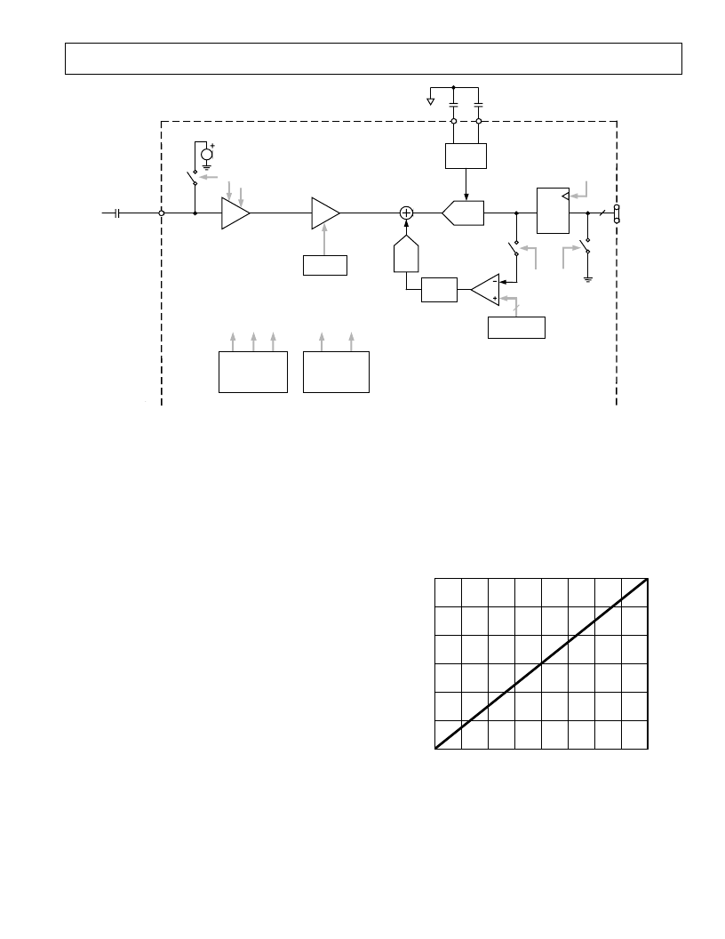
Figure 33. Analog Front End Functional Block Diagram
ANALOG FRONT END DESCRIPTION AND OPERATION
The AD9995 signal processing chain is shown in Figure 33.
Each processing step is essential in achieving a high quality image
from the raw CCD pixel data.
DC Restore
To reduce the large dc offset of the CCD output signal, a dc
restore circuit is used with an external 0.1 μF series coupling
capacitor. This restores the dc level of the CCD signal to
approximately 1.5 V, to be compatible with the 3 V supply
voltage of the AD9995.
Correlated Double Sampler
The CDS circuit samples each CCD pixel twice to extract the
video information and reject low frequency noise. The timing
shown in Figure 7 illustrates how the two internally generated
CDS clocks, SHP and SHD, are used to sample the reference
level and level of the CCD signal, respectively. The placement of
the SHP and SHD sampling edges is determined by the setting
of the SAMPCONTROL register located at Addr. 0x63. Place-
ment of these two clock signals is critical in achieving the best
performance from the CCD.
Variable Gain Amplifier
The VGA stage provides a gain range of 6 dB to 42 dB, program-
mable with 10-bit resolution through the serial digital interface.
The minimum gain of 6 dB is needed to match a 1 V input signal
with the ADC full-scale range of 2 V. When compared to 1 V
full-scale systems, the equivalent gain range is 0 dB to 36 dB.
The VGA gain curve follows a linear-in-dB characteristic. The
exact VGA gain can be calculated for any gain register value by
using the equation
0 0351
.
where the code range is 0 to 1023.
Gain dB
Code
dB
)
(
)
=
×
+
6
VGA GAIN REGISTER CODE
42
0
V
127
255
383
511
639
767
895
1023
36
30
24
18
12
6
Figure 34. VGA Gain Curve
REV. 0
相關PDF資料 |
PDF描述 |
|---|---|
| AD9995 | 12-Bit CCD Signal Processor with Precision Timing ⑩ Generator |
| ADA4000-2ARMZ-RL | Low Cost, Precision JFET Input Operational Amplifiers |
| ADA4000-1 | Low Cost, Precision JFET Input Operational Amplifiers |
| ADA4000-1_07 | Low Cost, Precision JFET Input Operational Amplifiers |
| ADA4000-1ARZ | Low Cost, Precision JFET Input Operational Amplifiers |
相關代理商/技術參數 |
參數描述 |
|---|---|
| AD9995KCPZ | 功能描述:IC CCD SIGNAL PROCESSOR 56-LFCSP RoHS:是 類別:集成電路 (IC) >> 接口 - 傳感器和探測器接口 系列:- 其它有關文件:Automotive Product Guide 產品培訓模塊:Lead (SnPb) Finish for COTS Obsolescence Mitigation Program 標準包裝:74 系列:- 類型:觸控式傳感器 輸入類型:數字 輸出類型:數字 接口:JTAG,串行 電流 - 電源:100µA 安裝類型:表面貼裝 封裝/外殼:20-TSSOP(0.173",4.40mm 寬) 供應商設備封裝:20-TSSOP 包裝:管件 |
| AD9995KCPZRL | 功能描述:IC CCD SIGNAL PROCESSOR 56-LFCSP RoHS:是 類別:集成電路 (IC) >> 接口 - 傳感器和探測器接口 系列:- 其它有關文件:Automotive Product Guide 產品培訓模塊:Lead (SnPb) Finish for COTS Obsolescence Mitigation Program 標準包裝:74 系列:- 類型:觸控式傳感器 輸入類型:數字 輸出類型:數字 接口:JTAG,串行 電流 - 電源:100µA 安裝類型:表面貼裝 封裝/外殼:20-TSSOP(0.173",4.40mm 寬) 供應商設備封裝:20-TSSOP 包裝:管件 |
| AD9995KCPZRL7 | 制造商:Rochester Electronics LLC 功能描述: 制造商:Analog Devices 功能描述: |
| AD9996BBCZ | 制造商:Rochester Electronics LLC 功能描述:14B 40 MSPS AFETG CONVERTER - Bulk |
| AD9996BBCZRL | 制造商:Rochester Electronics LLC 功能描述:- Bulk |
發布緊急采購,3分鐘左右您將得到回復。