- 您現(xiàn)在的位置:買賣IC網(wǎng) > PDF目錄373982 > ADF4193BCPZ (ANALOG DEVICES INC) Low Phase Noise, Fast Settling PLL Frequency Synthesizer PDF資料下載
參數(shù)資料
| 型號(hào): | ADF4193BCPZ |
| 廠商: | ANALOG DEVICES INC |
| 元件分類: | XO, clock |
| 英文描述: | Low Phase Noise, Fast Settling PLL Frequency Synthesizer |
| 中文描述: | PLL FREQUENCY SYNTHESIZER, 3500 MHz, QCC32 |
| 封裝: | 5 X 5 MM, ROHS COMPLIANT, MO-220VHHD-2, LFCSP-32 |
| 文件頁數(shù): | 13/28頁 |
| 文件大小: | 437K |
| 代理商: | ADF4193BCPZ |
第1頁第2頁第3頁第4頁第5頁第6頁第7頁第8頁第9頁第10頁第11頁第12頁當(dāng)前第13頁第14頁第15頁第16頁第17頁第18頁第19頁第20頁第21頁第22頁第23頁第24頁第25頁第26頁第27頁第28頁
ADF4193
Rev. B | Page 13 of 28
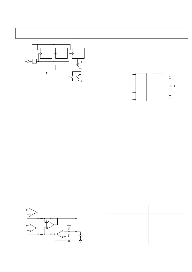
0
SW1/SW2
TIMEOUT
COUNTER
SW3
TIMEOUT
COUNTER
ICP
TIMEOUT
COUNTER
EN[64:1]
÷4
START
F
PFD
SW3
A
OUT
SW1
SW2
SW
GND
WRITE
TO R0
CHARGE PUMP
ENABLE LOGIC
Figure 25. Fast Lock Timeout Counters
Differential Amplifier
The internal, low noise, differential-to-single-ended amplifier is
used to convert the differential charge pump output to a single-
ended control voltage for the tuning port of the VCO. Figure 26
shows a simplified schematic of the differential amplifier. The
output voltage is equal to the differential voltage, offset by the
voltage on the CMR pin, according to
V
AOUT
= (
V
AIN+
V
AIN
) +
V
CMR
The CMR offset voltage is internally biased to three-fifths of
V
P
3, the differential amplifier power supply voltage, as shown in
Figure 26. Connect a 0.1 μF capacitor to ground to the CMR pin
to roll off the thermal noise of the biasing resistors.
As can be seen in Figure 15, the differential amplifier output
voltage behaves according to the previous equation over a 4 V
range from approximately 1.2 V minimum up to V
P
3 0.3 V.
However, fast settling is guaranteed only over a tuning voltage
range from 1.8 V up to V
P
3 0.8 V. This is to allow sufficient
room for overshoot in the PLL frequency settling transient.
Noise from the differential amplifier is suppressed inside the
PLL bandwidth. For loop bandwidths >20 kHz, the 1/f noise has
a negligible effect on the PLL output phase noise. Outside the
loop bandwidth, the differential amplifier’s noise FM modulates
the VCO. The passive filter network following the differential
amplifier, shown in Figure 36, suppresses this noise contribution to
below the VCO noise from offsets of 400 kHz and above. This
network has a negligible effect on lock time because it is
bypassed when SW3 is closed while the loop is locking.
0
AIN–
AOUT
AIN+
CMR
V
P
3
C EXT =
0.1μF
20k
30k
500
500
500
500
Figure 26. Differential Amplifier Block Diagram
MUX
OUT
and Lock Detect
The output multiplexer on the ADF4193 allows the user to
access various internal points on the chip. The state of MUX
OUT
is controlled by M4 to M1 in the MUX register. Figure 35 shows
the full truth table. Figure 27 shows the MUX
OUT
section in
block diagram form.
0
R DIVIDER OUTPUT
N DIVIDER OUTPUT
SERIAL DATA OUTPUT
D
GND
DV
DD
CONTROL
MUX
MUX
OUT
LOGIC LOW
THREE-STATE OUTPUT
TIMER OUTPUTS
DIGITAL LOCK DETECT
LOGIC HIGH
NOTE:
NOT ALL MUXOUT MODES SHOWN REFER TO MUX REGISTER
Figure 27. MUX
OUT
Circuit
Lock Detect
MUX
OUT
can be programmed to provide a digital lock detect
signal. Digital lock detect is active high. Its output goes high if
there are 40 successive PFD cycles with an input error of less
than 3 ns. For reliable lock detect operation with RF frequencies
<2 GHz, it is recommended that this threshold be increased to
10 ns by programming Register R6. The digital lock detect goes
low again when a new channel is programmed or when the
error at the PFD input exceeds 30 ns for one or more cycles.
Input Shift Register
The ADF4193 serial interface section includes a 24-bit input
shift register. Data is clocked in MSB first on each rising edge
of CLK. Data from the shift register is latched into one of eight
control registers, R0 to R7, on the rising edge of latch enable
(LE). The destination register is determined by the state of
the three control bits (Control Bit C3, Control Bit C2, and
Control Bit C1) in the shift register. The three LSBs are Bit DB2,
Bit DB1, and Bit DB0, as shown in the timing diagram of Figure 2.
The truth table for these bits is shown in Table 5. Figure 28
shows a summary of how the registers are programmed.
Table 5. C3, C2, and C1 Truth Table
Control Bits
C3
C2
C1
0
0
0
0
0
1
0
1
0
0
1
1
1
0
0
1
0
1
1
1
0
1
1
1
Name
FRAC/INT
MOD/R
Phase
Function
Charge Pump
Power-Down
Mux
Test Mode
Register
R0
R1
R2
R3
R4
R5
R6
R7
相關(guān)PDF資料 |
PDF描述 |
|---|---|
| ADF4193BCPZ-RL | Low Phase Noise, Fast Settling PLL Frequency Synthesizer |
| ADF4193BCPZ-RL7 | Low Phase Noise, Fast Settling PLL Frequency Synthesizer |
| ADF4207BRU | Dual RF PLL Frequency Synthesizers |
| ADF4208BRU | Dual RF PLL Frequency Synthesizers |
| ADF4206 | Dual RF PLL Frequency Synthesizers |
相關(guān)代理商/技術(shù)參數(shù) |
參數(shù)描述 |
|---|---|
| ADF4193BCPZ-RL | 功能描述:IC PLL FREQ SYNTHESIZER 32LFCSP RoHS:是 類別:集成電路 (IC) >> 時(shí)鐘/計(jì)時(shí) - 時(shí)鐘發(fā)生器,PLL,頻率合成器 系列:- 標(biāo)準(zhǔn)包裝:2,000 系列:- 類型:PLL 時(shí)鐘發(fā)生器 PLL:帶旁路 輸入:LVCMOS,LVPECL 輸出:LVCMOS 電路數(shù):1 比率 - 輸入:輸出:2:11 差分 - 輸入:輸出:是/無 頻率 - 最大:240MHz 除法器/乘法器:是/無 電源電壓:3.135 V ~ 3.465 V 工作溫度:0°C ~ 70°C 安裝類型:表面貼裝 封裝/外殼:32-LQFP 供應(yīng)商設(shè)備封裝:32-TQFP(7x7) 包裝:帶卷 (TR) |
| ADF4193BCPZ-RL7 | 功能描述:IC PLL FREQ SYNTHESIZER 32LFCSP RoHS:是 類別:集成電路 (IC) >> 時(shí)鐘/計(jì)時(shí) - 時(shí)鐘發(fā)生器,PLL,頻率合成器 系列:- 標(biāo)準(zhǔn)包裝:2,000 系列:- 類型:PLL 時(shí)鐘發(fā)生器 PLL:帶旁路 輸入:LVCMOS,LVPECL 輸出:LVCMOS 電路數(shù):1 比率 - 輸入:輸出:2:11 差分 - 輸入:輸出:是/無 頻率 - 最大:240MHz 除法器/乘法器:是/無 電源電壓:3.135 V ~ 3.465 V 工作溫度:0°C ~ 70°C 安裝類型:表面貼裝 封裝/外殼:32-LQFP 供應(yīng)商設(shè)備封裝:32-TQFP(7x7) 包裝:帶卷 (TR) |
| ADF4193SP1BCPZ | 制造商:Analog Devices 功能描述: |
| ADF4193SP1BCPZ-RL7 | 制造商:Analog Devices 功能描述: |
| ADF4193SP2BCPZ-RL7 | 制造商:Analog Devices 功能描述: |
發(fā)布緊急采購,3分鐘左右您將得到回復(fù)。